Circuit board and manufacturing method thereof

A manufacturing method and circuit board technology, applied in the directions of printed circuit manufacturing, multilayer circuit manufacturing, printed circuit, etc., can solve the problems of exceeding the height of the conductive medium, the non-drilling layer of the multilayer circuit board, and the insertion loss of the multilayer circuit board. , to ensure the effect of insertion loss

Inactive Publication Date: 2021-05-21
SHENNAN CIRCUITS
View PDF3 Cites 0 Cited by
  • Summary
  • Abstract
  • Description
  • Claims
  • Application Information

AI Technical Summary

Problems solved by technology

[0004] The present application provides a circuit board to solve the problem that the back-drilling process in the prior art easily leads to the height of the conductive medium in the conductive via hole between the non-drillable layer and the adjacent must-drillable layer of the multilayer circuit board Exceeding the preset range, resulting in the problem that the insertion loss of the multilayer circuit board is too high

Method used


Image

  • Circuit board and manufacturing method thereof
  • Circuit board and manufacturing method thereof
  • Circuit board and manufacturing method thereof

Examples


Embodiment Construction

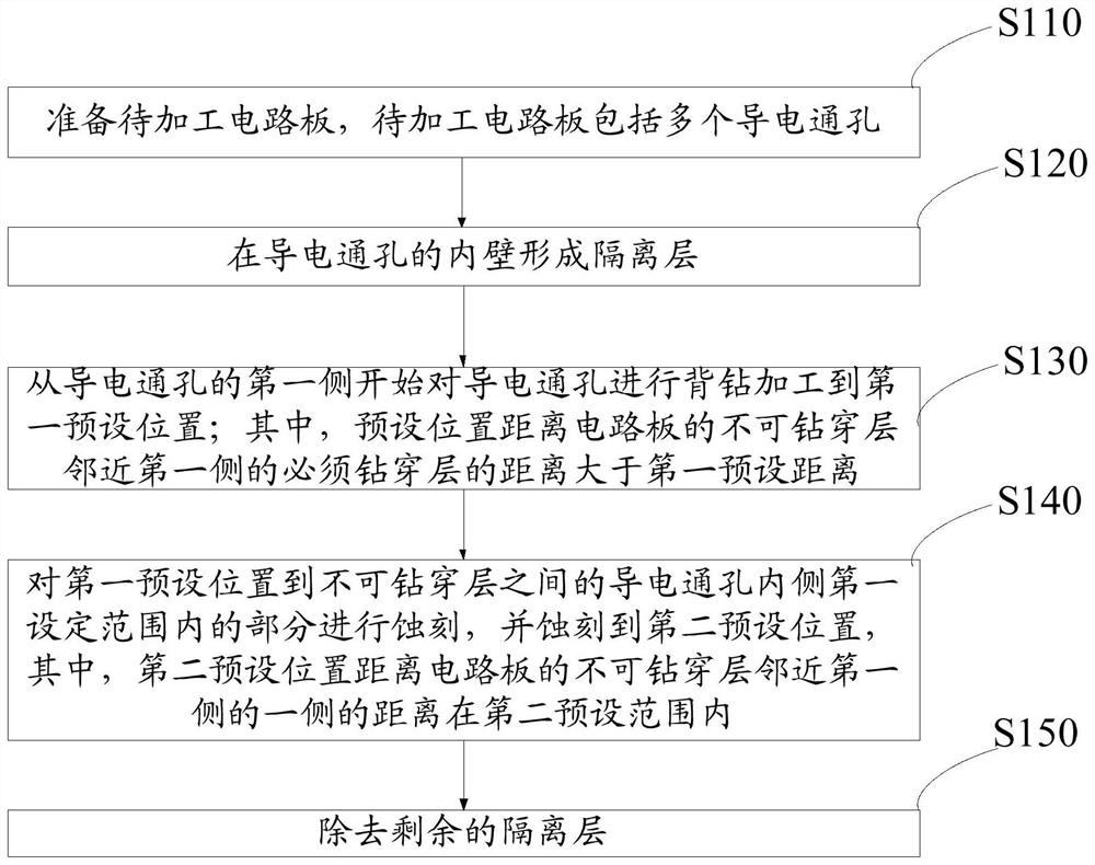
[0036] In order to make the technical problems solved by the present application, the technical solutions adopted and the technical effects achieved clearer, the technical solutions of the embodiments of the present application will be further described in detail below in conjunction with the accompanying drawings.

[0037] Reference herein to an "embodiment" means that a particular feature, structure, or characteristic described in connection with the embodiment can be included in at least one embodiment of the present application. The occurrences of this phrase in various places in the specification are not necessarily all referring to the same embodiment, nor are separate or alternative embodiments mutually exclusive of other embodiments. It is understood explicitly and implicitly by those skilled in the art that the embodiments described herein can be combined with other embodiments.

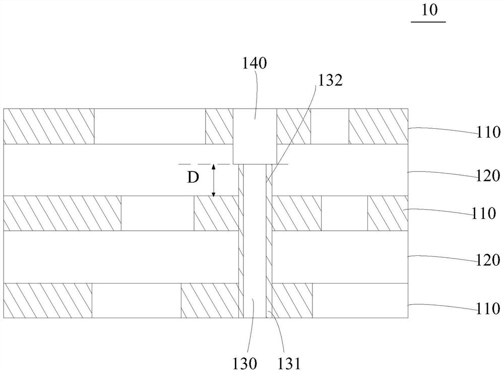
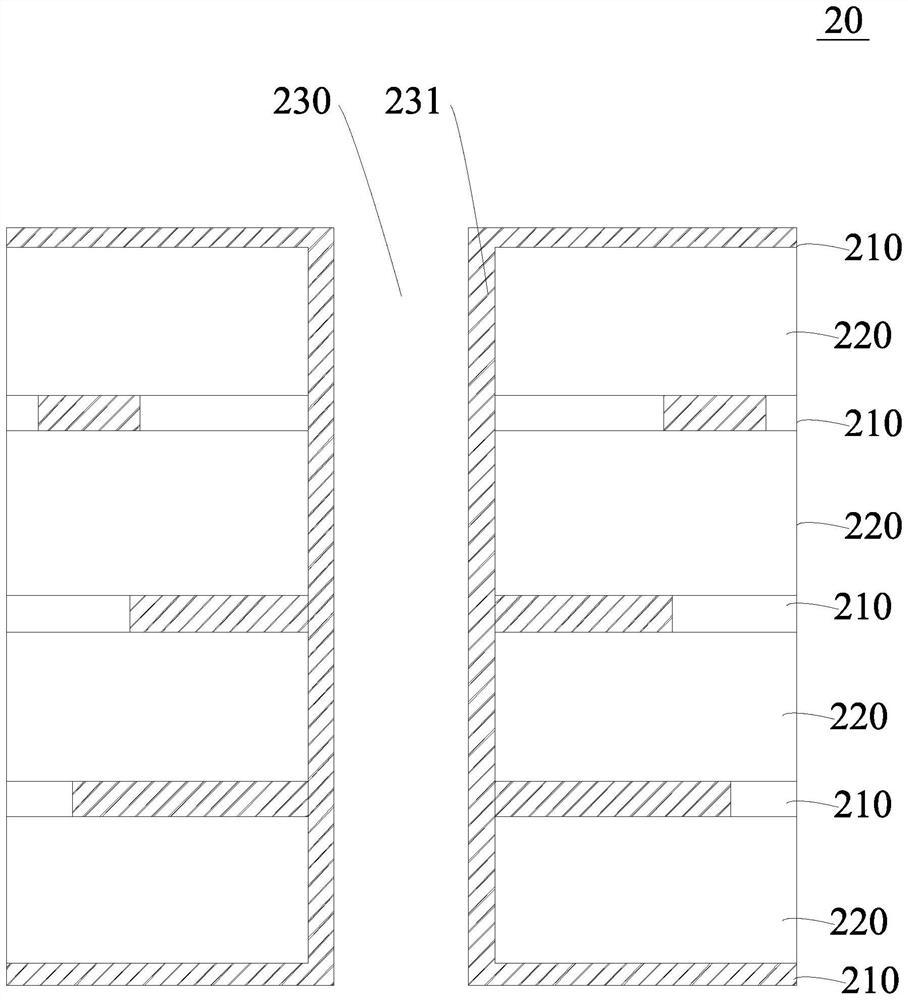
[0038] In the existing multilayer circuit board processing process, it is usually necess...


PUM


Abstract

The invention discloses a circuit board and a manufacturing method thereof. The manufacturing method of the circuit board comprises the following steps: preparing a circuit board to be processed, wherein the circuit board to be processed comprises a plurality of conductive through holes; forming isolation layers on the inner walls of the conductive through holes; performing back drilling processing on each conductive through hole from the first side of the conductive through hole to a first preset position, wherein the distance between the first preset position and the layer, which must be drilled, of the non-drillable layer of the circuit board and is adjacent to the first side is greater than the first preset distance; and etching a part in a first set range on the inner side of the conductive through hole between the first preset position and the non-drillable layer to a second preset position, the distance between the second preset position and one side, adjacent to the first side, of the non-drillable layer of the circuit board being within a second preset range. By means of the scheme, it can be ensured that the insertion loss of the manufactured circuit board is within the preset range.

Description

technical field [0001] The present application relates to the technical field of circuit boards, in particular to a circuit board and a manufacturing method thereof. Background technique [0002] In the production of existing multi-layer circuit boards, it is usually necessary to adopt a back-drilling process to form a back-drilled hole on the basis of the conductive via hole of the multi-layer circuit board, so that the inner layer circuit connected to the back-drilled hole is in the The location of the back-drilled hole is usually used to disconnect the electrical connection, so that the multi-layer conductive layers of the multi-layer circuit board can be formed into a functional circuit. [0003] Existing back drilling generally uses mechanical drilling to expand the conductive vias to remove the conductive medium in the conductive vias. Due to the thickness deviation of the multilayer circuit board in production, it may cause After the back drilling is formed, the heig...

Claims


Application Information

Patent Timeline
Patent Type & Authority Applications(China)
IPC IPC(8): H05K3/46H05K3/42H05K1/02H05K1/11
CPCH05K1/0298H05K1/116H05K3/429H05K3/46H05K3/4644
Inventor 李智韩雪川崔荣
Owner SHENNAN CIRCUITS
Why Eureka
Try Eureka