A novel microwave probe contact sheet and its manufacturing method

A manufacturing method and a technology of a contact sheet, which are applied in the field of microwave probes, can solve the problems of difficult removal of the contact surface, high processing difficulty, and high processing cost, and achieve the effects of reducing sliding friction, reducing processing difficulty, and reducing processing cost

Active Publication Date: 2022-08-02
CHINA ELECTRONIS TECH INSTR CO LTD
View PDF8 Cites 0 Cited by
  • Summary
  • Abstract
  • Description
  • Claims
  • Application Information

AI Technical Summary

Problems solved by technology

[0003] The contact surface 6 of the existing microwave probe contact piece and the pad of the bare chip is a planar structure, and it is difficult to keep absolutely parallel between the contact surface 6 and the pad of the bare chip, which causes the contact piece to cause certain damage to the pad of the bare chip during the test. damage, especially when multiple contacts are required to be in contact with the die pad at the same time, there will always be a contact that touches the die pad first, and the microwave probe continues to exert pressure so that the remaining contacts can contact the die pad During the process, sliding on the pad causes scratches to the pad
[0004] The top of the existing microwave probe contact sheet needs to be formed with 3 slopes, such as figure 1 a. figure 1 b and figure 2 a. figure 2 As shown in b, the three slopes (contact surface 6, slope one 7, slope two 8) are distributed on the front and back surfaces of the contact piece. During processing, it is necessary to ensure the slope angle requirements and minimize the contact piece processing process The deformation and damage in the contact surface are very difficult to process and the processing cost is high; at present, traditional machining methods are used, and the processing residual burrs on the contact surface are also difficult to remove, which affects the electrical performance indicators such as insertion loss and voltage standing wave ratio of the probe.

Method used


Image

  • A novel microwave probe contact sheet and its manufacturing method
  • A novel microwave probe contact sheet and its manufacturing method
  • A novel microwave probe contact sheet and its manufacturing method

Examples


Embodiment Construction

[0048] The technical solutions in the embodiments of the present invention will be clearly and completely described below with reference to the accompanying drawings in the embodiments of the present invention.

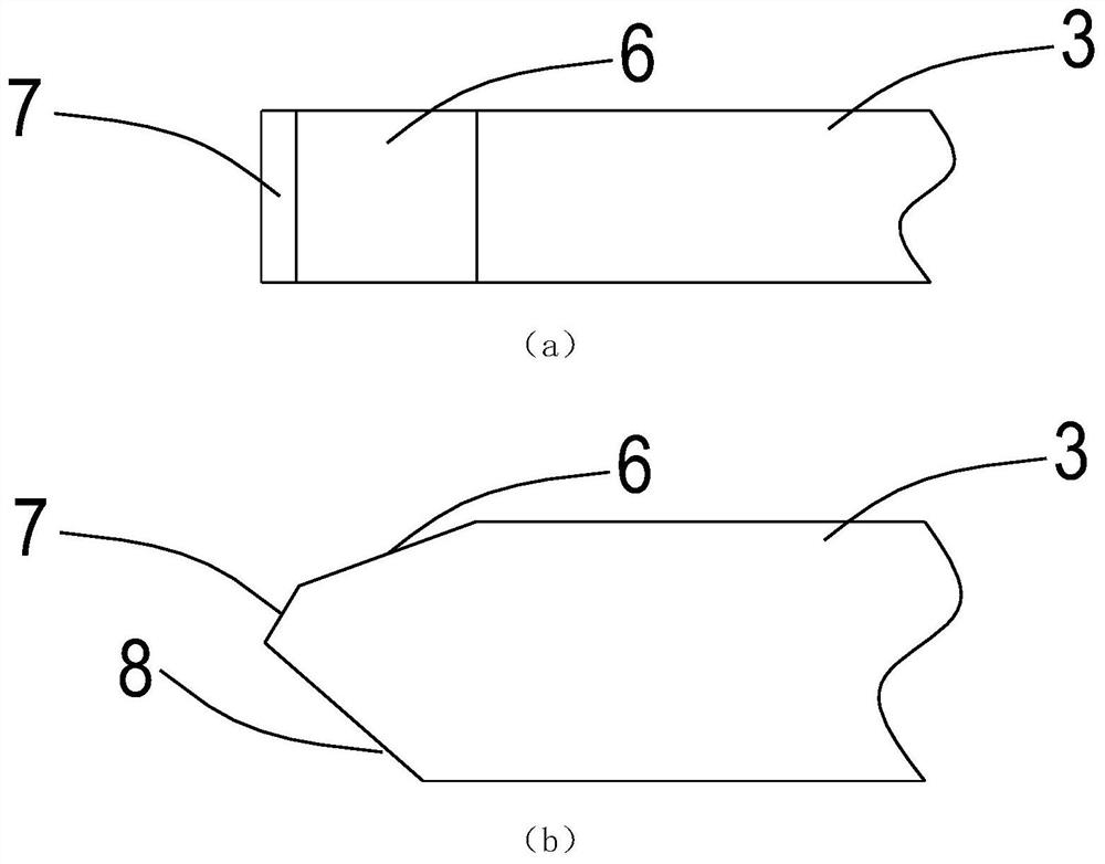
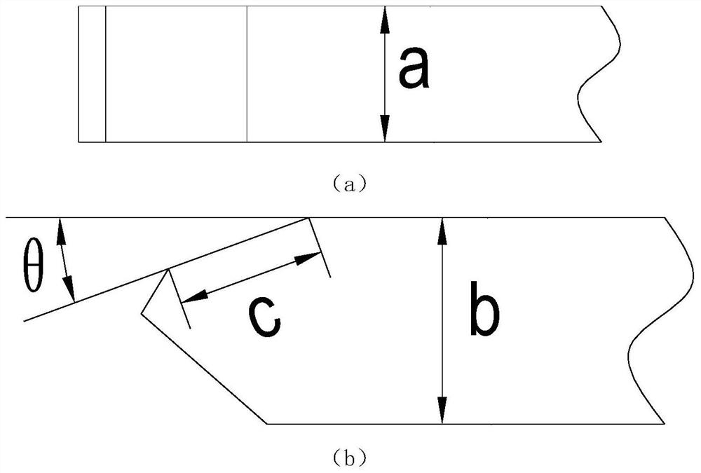
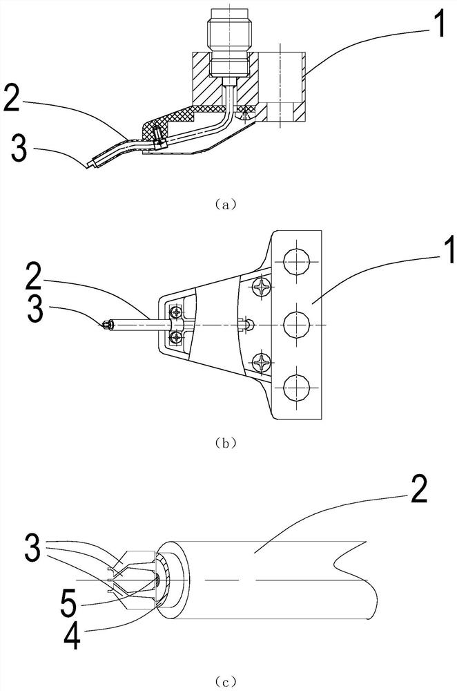
[0049] The invention provides a novel microwave probe contact piece, which comprises a plurality of parallel contact pieces arranged at the front end of the coaxial cable. The bottom surface of the front end of each contact piece is an elliptical arc surface, and the top surface of the front end is Inwardly concave bevel. Taking a certain type of GSG microwave probe as an example, the technical solution of the present invention is described, and its structural diagram is as follows image 3 a and image 3 As shown in b, the probe consists of a base 1, a coaxial cable 2 and a contact piece 3. Among them, the G terminal of the contact piece is assembled on the outer conductor 4 of the coaxial cable, and the S terminal is assembled on the inner conductor 5 of the coaxi...


PUM

PropertyMeasurementUnit
thicknessaaaaaaaaaa
thicknessaaaaaaaaaa

Abstract

The invention discloses a novel microwave probe contact piece and a manufacturing method thereof. The contact piece comprises a plurality of split contact pieces arranged in parallel on the front end of a coaxial cable, and the bottom surface of the front end of each contact piece is an elliptical arc. The top surface of the front end is an inwardly concave slope. The novel microwave probe contact sheet disclosed by the invention changes the contact surface from a flat surface to an elliptical arc surface, reduces the sliding friction force when the contact surface is in contact with the bare chip pad, and causes little damage to the bare chip pad; the invention The top of the proposed contact surface only needs one bevel to be processed and formed, which greatly reduces the processing difficulty and processing cost, and the bevel is on the back of the contact surface. The pieces maintain their respective shapes and mutual positional relationship before being welded to the coaxial cable, and the connection part is removed after welding, which can effectively ensure the shape and position tolerance of each split contact piece, thereby ensuring the electrical performance indicators such as the insertion loss of the contact piece.

Description

technical field [0001] The invention relates to a microwave probe, in particular to a novel microwave probe contact sheet and a manufacturing method thereof. Background technique [0002] With the development of electronic technology and the growth of demand, higher requirements are placed on the frequency and bandwidth of microwave testing, and the testing of microwave and millimeter-wave bare chips is one of the important requirements. Because these chips have the characteristics of small geometric size, circuit feature size reaching sub-micron level and below, and easy damage, they need a special testing device - microwave probe to achieve. According to demand, microwave probes are divided into GS, SG, GSG, GSGSG, GSGS, GSS, GSSG, SGS, SGSG and SSG and other types, all types without exception use contact pads and bare chip pads for contact type Measurement. The contact piece is assembled with the coaxial cable, the contact piece terminal assembled with the inner conduct...

Claims


Application Information

Patent Timeline
Patent Type & Authority Patents(China)
IPC IPC(8): G01R1/067G01R31/28
CPCG01R1/06711G01R31/2863
Inventor 王斌葛新灵付延新桑锦正宋振国路波
Owner CHINA ELECTRONIS TECH INSTR CO LTD
Why Eureka
Try Eureka