Two-dimensional rapid iteration method and device for electromagnetic response of three-dimensional large-scale integrated circuit

A large-scale integrated circuit and integrated circuit technology, applied in 3D modeling, electrical digital data processing, special data processing applications, etc., can solve problems such as long calculation time, increasing the number of non-zero elements of sparse matrices, and the complexity of solving sparse matrices

Active Publication Date: 2021-05-25
北京智芯仿真科技有限公司
View PDF7 Cites 8 Cited by
  • Summary
  • Abstract
  • Description
  • Claims
  • Application Information

AI Technical Summary

Problems solved by technology

Since the method of moments only integrates for the interface, it will reduce a large number of grid units and unknown quantities. However, since the scale of integrated circuits ranges from nanometers to centimeters, directly solving the whole integrated circuit with the finite element method itself will cause problems. Huge sparse matrix, and due to the coupling of the finite element method and the method of moments, the formed coupling matrix is ​​a dense matrix at the interface, which greatly increases the number of non-zero elements of the entire sparse matrix and the complexity of the sparse matrix solution, making the calculation time still very long

Method used


Image

  • Two-dimensional rapid iteration method and device for electromagnetic response of three-dimensional large-scale integrated circuit
  • Two-dimensional rapid iteration method and device for electromagnetic response of three-dimensional large-scale integrated circuit
  • Two-dimensional rapid iteration method and device for electromagnetic response of three-dimensional large-scale integrated circuit

Examples


Embodiment Construction

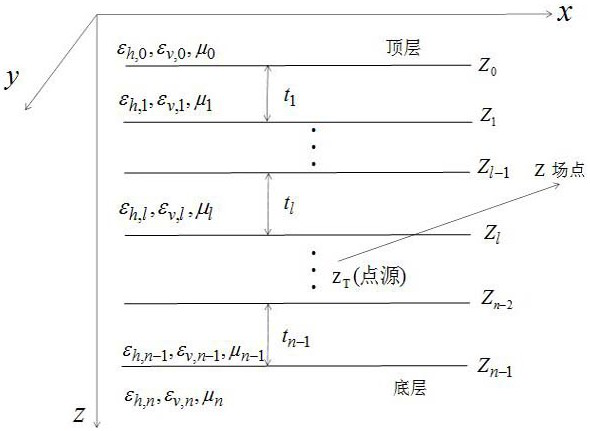
[0057] In order to make the objectives, technical solutions and advantages of the present invention clearer, the technical solutions in the embodiments of the present invention will be described in more detail below in conjunction with the drawings in the embodiments of the present invention.

[0058] It should be noted that: in the drawings, the same or similar symbols represent the same or similar elements or elements with the same or similar functions. The described embodiments are part of the embodiments of the present invention, but not all of the embodiments. In the case of no conflict, the embodiments in the present application and the features in the embodiments can be combined with each other. Based on the embodiments of the present invention, all other embodiments obtained by persons of ordinary skill in the art without creative efforts fall within the protection scope of the present invention.

[0059] In describing the present invention, it is to be understood that...


PUM


Abstract

The invention provides a two-dimensional rapid iteration method for electromagnetic response of a three-dimensional large-scale integrated circuit. The two-dimensional rapid iteration method comprises the following steps: 1, dividing each layer of integrated circuit layout with a complex shape into polygons with simple shapes; 2, taking the influence of other layers as an additional source, and calculating the electromagnetic field and surface current distribution of each layer of the integrated circuit layout through a two-dimensional finite element method; 3, calculating the influence of the non-uniformly distributed surface current on the simple-shaped polygon on the field points through two-dimensional Gaussian integral based on a vector Green function of the influence of a point current source on the field points, and further calculating the influence of the non-uniformly distributed surface current on the complex-shaped integrated circuit layout on the electromagnetic field distribution of all other layers; and 4, judging whether the change quantity of the electromagnetic field distribution of all layers is smaller than a preset error threshold value or not, if yes, ending, and if not, turning to the step 2. The invention further provides a device of the method, and the electromagnetic response on the three-dimensional integrated circuit layout can be rapidly calculated through two-dimensional iteration.

Description

technical field [0001] The invention relates to the technical field of integrated circuits, in particular to a two-dimensional rapid iteration method and device for electromagnetic response of three-dimensional large-scale integrated circuits. Background technique [0002] With the development of communication technology, the research and development of VLSI has gradually started. In order to improve the performance of electronic equipment, reduce the size and reduce the cost, transistors, other components and circuits are integrated on a small semiconductor substrate. In order to achieve more functions, VLSI has a structure of several to hundreds of layers, and each layer has an extremely complex structure, integrating millions or even tens of millions of transistors. It has a multi-scale structure, from the centimeter level to the latest nanometer level. Such a complex structure also brings difficulties to its electromagnetic field analysis. [0003] When using the trad...

Claims


Application Information

Patent Timeline
Patent Type & Authority Applications(China)
IPC IPC(8): G06F30/398G06T17/20
CPCG06T17/20G06F30/398
Inventor 唐章宏邹军王芬黄承清汲亚飞
Owner 北京智芯仿真科技有限公司
Why Eureka
Try Eureka