Photoelectronic component wafer collecting device

A technology for optoelectronic components and collection equipment, which is applied in the manufacturing of electrical components, circuits, semiconductor/solid-state devices, etc. The effect of work efficiency

Pending Publication Date: 2021-05-28
江苏晶曌半导体有限公司
View PDF0 Cites 0 Cited by
  • Summary
  • Abstract
  • Description
  • Claims
  • Application Information

AI Technical Summary

Problems solved by technology

[0003] At present, during the production and collection of traditional optoelectronic element wafers, it is necessary to conduct preliminary manual screening of optoelectronic element wafers to separate unqualified optoelectronic element wafers. It is very troublesome to operate and the work efficiency is low

Method used


Image

  • Photoelectronic component wafer collecting device
  • Photoelectronic component wafer collecting device

Examples


Embodiment Construction

[0016] The following will clearly and completely describe the technical solutions in the embodiments of the present invention with reference to the accompanying drawings in the embodiments of the present invention. Obviously, the described embodiments are only some, not all, embodiments of the present invention. Based on the embodiments of the present invention, all other embodiments obtained by persons of ordinary skill in the art without making creative efforts belong to the protection scope of the present invention.

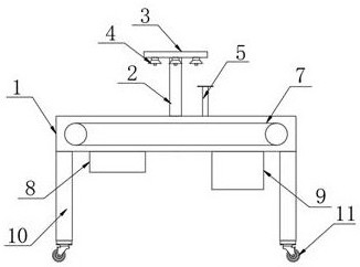
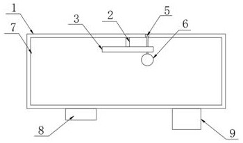
[0017] The present invention provides such Figure 1-2 The one shown is used for collecting wafers of optoelectronic components, including a workbench 1, a vertical pole 2 is fixedly connected to the rear side of the top of the workbench 1, and a crossbar 3 is fixedly connected to the top side of the support pole. The bottom of the rod 3 is fixedly connected with a lighting lamp 4, the top rear side of the workbench 1 is connected with a support frame 5 by bol...


PUM


Abstract

The invention discloses a photoelectronic component wafer collecting device, and particularly relates to the technical field of photoelectronic component production. The photoelectronic component wafer collecting device comprises a workbench, a vertical rod is fixedly connected to the rear side of the top of the workbench, a transverse rod is fixedly connected to one side of the top of a support rod, an illuminating lamp is fixedly connected to the bottom of the transverse rod, a supporting frame is connected to the rear side of the top of the workbench through bolts, a magnifying lens is fixedly connected to one side of the top of the supporting frame, a conveying belt is arranged in the workbench, through holes are formed in the two sides of the inner wall of the workbench, and the through holes are rotationally connected with the conveying belt through bearings. According to the photoelectronic component wafer collecting device, optoelectronic component wafers are conveyed through the conveying belt, an operator can inspect the optoelectronic component wafers through the magnifying lens, the good optoelectronic component wafers are placed in a finished product collecting box after inspection, the bad optoelectronic component wafers are placed in a waste collecting box, the operator is prevented from taking and placing the optoelectronic component wafers many times, and the working efficiency is improved.

Description

technical field [0001] The invention relates to the technical field of optoelectronic device production, and more specifically, the invention relates to a wafer collection device for optoelectronic components. Background technique [0002] Optoelectronic devices mainly include light sources as information carriers, radiation detectors, components for control and processing, optical fibers, and display and imaging devices. As a light source for information carriers, the process of thermal radiation is difficult to control quickly, but the beam emitted by it can be modulated, filtered or otherwise processed to make the beam carry information on the way. Luminous light sources other than thermal radiation can naturally also carry information during the transmission process, but more importantly, they carry information during the emission process. Generally, semiconductor PN junction light-emitting diodes that can be driven by low voltage are used, especially high-brightness se...

Claims


Application Information

Patent Timeline
IPC IPC(8): B07C7/04H01L21/67
CPCB07C7/04H01L21/67271
Inventor 不公告发明人
Owner 江苏晶曌半导体有限公司
Why Eureka
Try Eureka