Gate layer manufacturing method, semiconductor device manufacturing method and semiconductor construction

A manufacturing method and semiconductor technology, applied in semiconductor/solid-state device manufacturing, semiconductor devices, electrical components, etc., can solve problems such as increased leakage current, threshold voltage drift of metal oxide semiconductor devices, large energy and energy, etc., to achieve improved Yield rate, avoiding multiple handling or transmission, and improving stability

Active Publication Date: 2013-05-29
SEMICON MFG INT (SHANGHAI) CORP +1
View PDF1 Cites 0 Cited by
  • Summary
  • Abstract
  • Description
  • Claims
  • Application Information

AI Technical Summary

Problems solved by technology

[0009] In the process of using doped polysilicon to form the gate, the energy and energy of ion implantation during doping are very large, the implanted energy can reach 5KeV to 15KeV, and the dose can reach 2×10 15 atom / cm 2 up to 5×10 15 atom / cm 2 , the implanted ions will enter or penetrate the gate insulating layer, causing electrical problems such as threshold voltage drift and leakage current increase of the metal oxide semiconductor device formed.

Method used


Image

  • Gate layer manufacturing method, semiconductor device manufacturing method and semiconductor construction
  • Gate layer manufacturing method, semiconductor device manufacturing method and semiconductor construction
  • Gate layer manufacturing method, semiconductor device manufacturing method and semiconductor construction

Examples


Embodiment Construction

[0053] The specific embodiments of the present invention will be described in detail below in conjunction with the accompanying drawings.

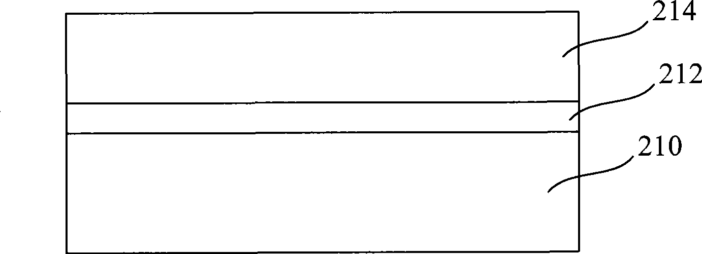
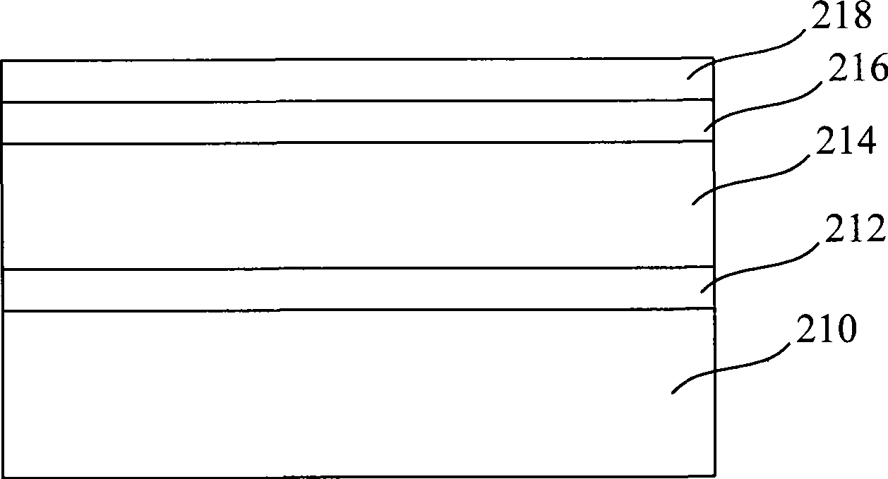
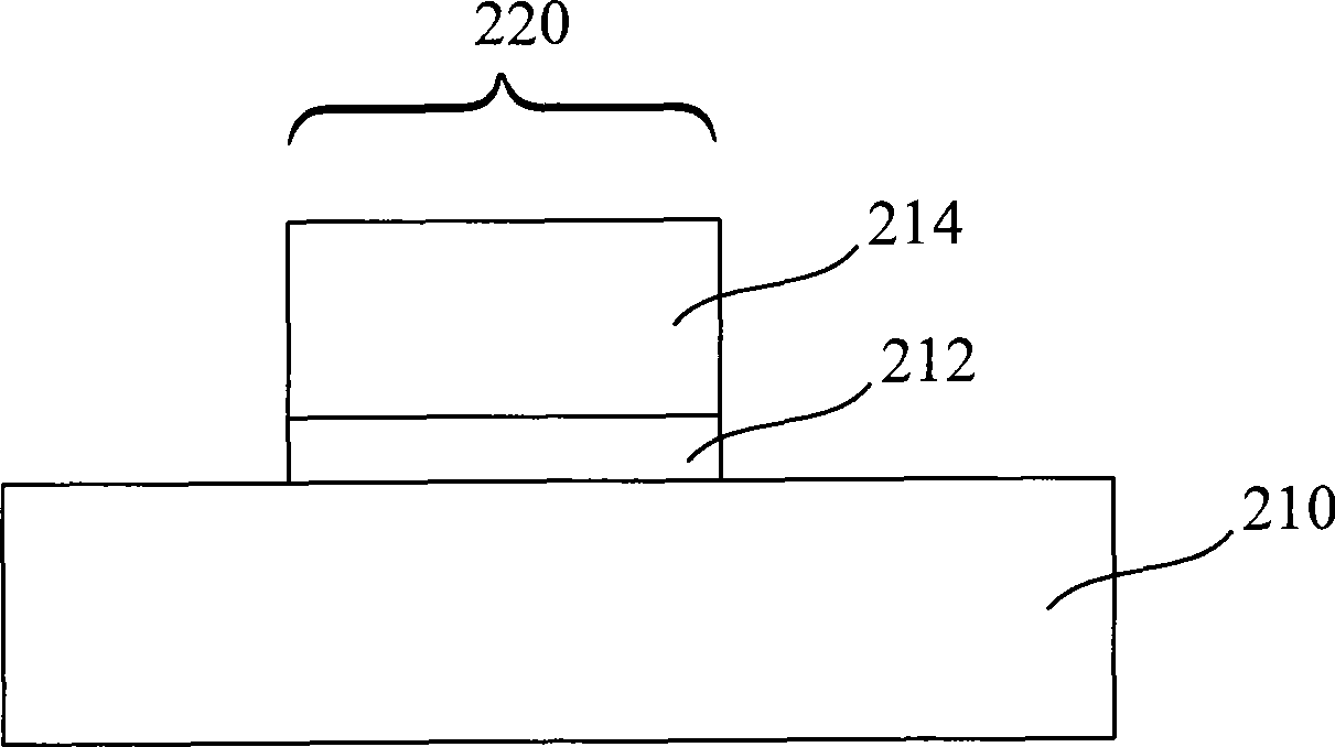
[0054] With the continuous development of the semiconductor manufacturing process, the size of the gate is getting smaller and smaller. In order to ensure the fast response and low power consumption of the formed semiconductor device, it is necessary to reduce the resistance of the gate. One of the methods is to form a polysilicon gate. During ion implantation, polysilicon is doped by ion implantation; however, during ion implantation, due to the high energy of the implanted ions, the implanted ions will pass through the gate insulating layer and enter the conductive channel.

[0055] The invention provides a method for manufacturing a gate layer. When forming a polysilicon gate layer for manufacturing a gate, at least one polysilicon layer in which crystal grains are randomly arranged (or distributed) is formed in the gate layer, and the p...


PUM


Abstract

A manufacturing method of a grid layer comprises the steps of providing a semiconductor substrate with a grid electrode insulating layer; forming a first polycrystalline silicon layer on the semiconductor substrate; forming a second polycrystalline silicon layer with randomly distributed crystal grains; and carrying out ion implantation doping to the second and the first polycrystalline silicon layers. The invention also provides a manufacturing method of a semiconductor device, and a semiconductor structure. The method can prevent or reduce doping ions from entering into or passing through the grid electrode insulating layer when carrying out ion implantation doping to the grid electrode layers.

Description

technical field [0001] The invention relates to the technical field of semiconductor manufacturing, in particular to a manufacturing method of a gate layer, a manufacturing method of a semiconductor device and a semiconductor structure. Background technique [0002] With the continuous improvement of semiconductor manufacturing technology, the integration level is getting higher and higher, and the critical dimension of the gate representing the level of semiconductor manufacturing technology is getting smaller and smaller; in metal oxide semiconductor transistors, polysilicon is generally used as the material for manufacturing the gate , Moreover, in order to reduce power consumption and improve response speed, polysilicon is often doped to form doped polysilicon to reduce the resistance of the gate, for example, for the polysilicon gate of an N-type metal oxide semiconductor transistor (NMOS), N-type impurities are doped, and for the polysilicon gate of a P-type metal oxid...

Claims


Application Information

Patent Timeline
Patent Type & Authority Patents(China)
IPC IPC(8): H01L21/28H01L21/336H01L29/49H01L29/78
Inventor 何永根陈旺
Owner SEMICON MFG INT (SHANGHAI) CORP
Why Eureka
Try Eureka