Supercharge Your Innovation With Domain-Expert AI Agents!

Display panel, manufacturing method thereof and mask plate

A technology for display panels and motherboards, applied in nonlinear optics, instruments, optics, etc., can solve the problems of test vias remaining in the other adjacent one, poor display of black matrix layer, etc., to avoid product defects Effect

Active Publication Date: 2021-05-28
FUZHOU BOE OPTOELECTRONICS TECH CO LTD +1
View PDF5 Cites 0 Cited by
  • Summary
  • Abstract
  • Description
  • Claims
  • Application Information

AI Technical Summary

Problems solved by technology

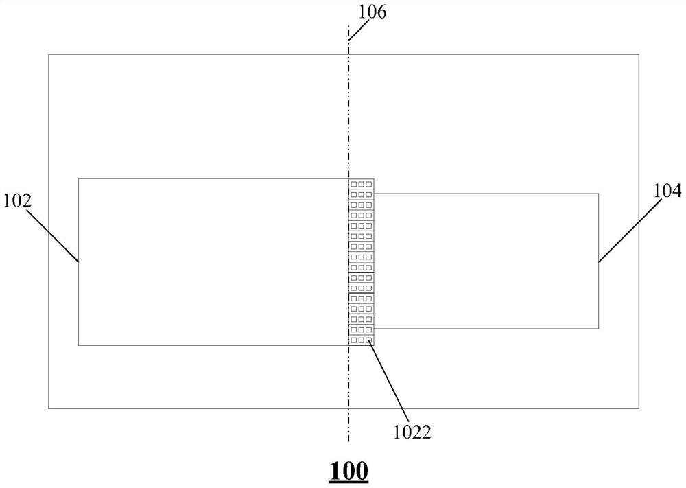
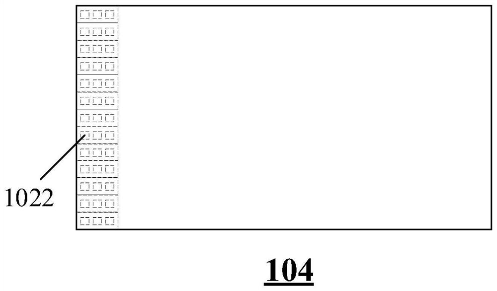
Therefore, in order to improve the utilization rate of the substrate and reduce the production cost, in the display motherboard, a zero-cut design is often required between adjacent display panels, that is, the cutting line for cutting the display motherboard is aligned with the edge of the display panel. As a result, in some cases, the test via hole (2D Via) of some display panels will remain on the edge of another display panel adjacent to it
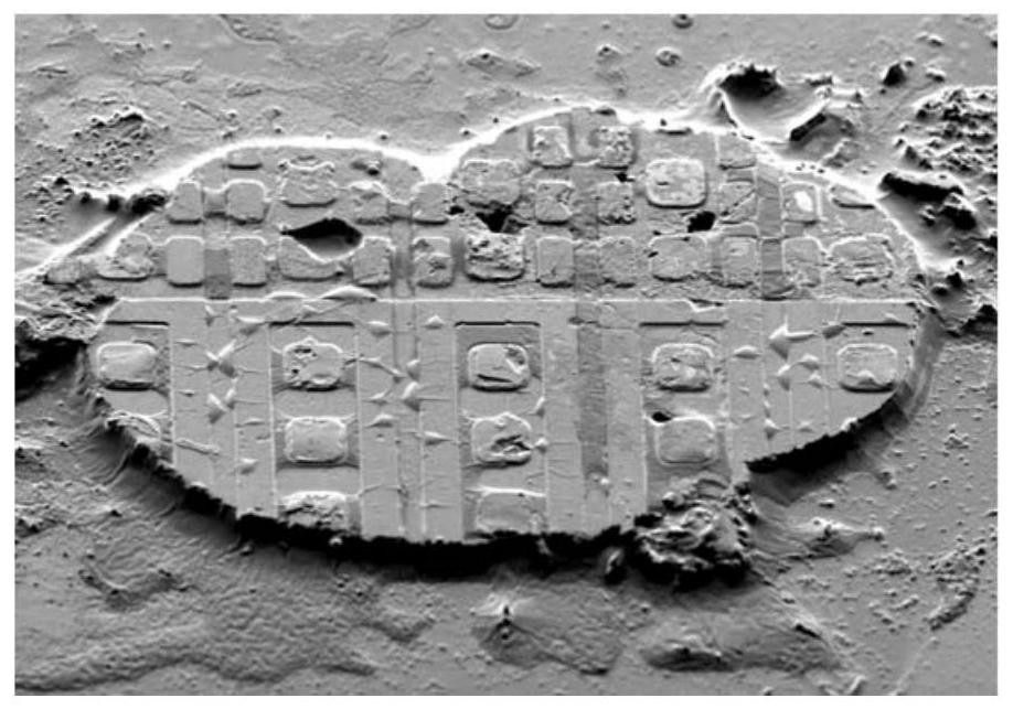
The remaining test vias will be corroded by water vapor and then charged, and the charge will be transferred to the black matrix layer (BM) on the opposite color filter substrate, which will cause the black matrix layer to be charged and cause poor display

Method used


Image

  • Display panel, manufacturing method thereof and mask plate
  • Display panel, manufacturing method thereof and mask plate
  • Display panel, manufacturing method thereof and mask plate

Examples


Embodiment Construction

[0035] In order to make the purpose, technical solutions and advantages of the present disclosure clearer, the present disclosure will be further described in detail below in conjunction with specific embodiments and with reference to the accompanying drawings.

[0036] It should be noted that, unless otherwise defined, the technical terms or scientific terms used in the embodiments of the present disclosure shall have ordinary meanings understood by those skilled in the art to which the present disclosure belongs. "First", "second" and similar words used in the embodiments of the present disclosure do not indicate any sequence, quantity or importance, but are only used to distinguish different components. "Comprising" or "comprising" and similar words mean that the elements or items appearing before the word include the elements or items listed after the word and their equivalents, without excluding other elements or items. Words such as "connected" or "connected" are not lim...


PUM


Abstract

The invention provides a display panel, a manufacturing method thereof and a mask plate. The display panel comprises an array substrate and a color film substrate, wherein one surface, facing the color film substrate, of the array substrate is provided with a through hole for testing; an isolating layer corresponding to the through hole for testing is arranged on one surface, facing the array substrate, of the color film substrate; and the orthographic projection of the through hole for testing on the color film substrate is located in the isolating layer, and the isolating layer is made of an insulating material.

Description

technical field [0001] The present disclosure relates to the field of display technology, and in particular to a display panel, a manufacturing method thereof, and a mask plate. Background technique [0002] In the context of increasingly fierce competition in the liquid crystal display industry, effectively reducing costs can significantly improve product competitiveness, and improving the utilization rate of substrates (eg, glass substrates) is one of the effective ways to reduce costs. Therefore, in order to improve the utilization rate of the substrate and reduce the production cost, in the display motherboard, a zero-cut design is often required between adjacent display panels, that is, the cutting line for cutting the display motherboard is aligned with the edge of the display panel, As a result, in some cases, the test via hole (2D Via) of some display panels will remain on the edge of another adjacent display panel. The remaining via holes for testing will be corrod...

Claims


Application Information

Patent Timeline
Patent Type & Authority Applications(China)
IPC IPC(8): G02F1/1362G02F1/1335
CPCG02F1/1362G02F1/133512
Inventor 陈小龙方鑫王金良王文超周志伟
Owner FUZHOU BOE OPTOELECTRONICS TECH CO LTD
Features
  • R&D
  • Intellectual Property
  • Life Sciences
  • Materials
  • Tech Scout
  • Unparalleled Data Quality
  • Higher Quality Content
  • 60% Fewer Hallucinations
Learn More