Film transistor and preparation method thereof, array substrate and display panel

A thin-film transistor and thin-film technology, which is applied in the direction of transistor, semiconductor/solid-state device manufacturing, nanotechnology for materials and surface science, etc., can solve the problem that the active layer is easy to be corroded, so as to avoid defective devices and realize simple process , The effect of simple process

Inactive Publication Date: 2015-09-23
BOE TECH GRP CO LTD +1
View PDF5 Cites 27 Cited by
  • Summary
  • Abstract
  • Description
  • Claims
  • Application Information

AI Technical Summary

Problems solved by technology

[0005] The purpose of the present invention is to provide a thin film transistor and its preparation method, an array substrate and a display panel to solve the problem that the active layer is easily corroded when the metal oxide thin film transistor is prepared by the back channel etching process in the prior art

Method used


Image

  • Film transistor and preparation method thereof, array substrate and display panel
  • Film transistor and preparation method thereof, array substrate and display panel
  • Film transistor and preparation method thereof, array substrate and display panel

Examples


preparation example Construction

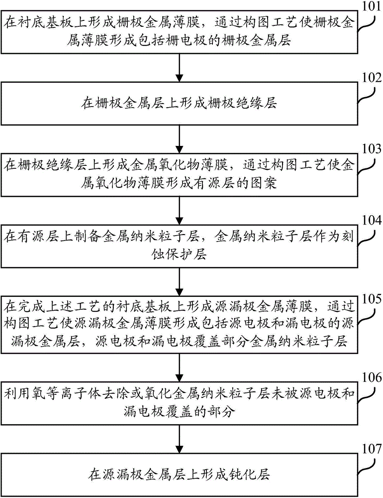
[0051] see figure 1 , an embodiment of the present invention provides a method for manufacturing a thin film transistor, including:

[0052] 101. Form a gate metal thin film on a base substrate, and form the gate metal thin film into a gate metal layer including a gate electrode through a patterning process.

[0053] Depending on the specific application of the metal oxide thin film transistor, a glass substrate with a buffer layer can be used as the base substrate, or a flexible substrate with a water-oxygen barrier layer can be used as the base substrate, preferably, polyethylene naphthalate Glycol ester, polyethylene terephthalate, polyimide, or metal foil are used as materials for the flexible substrate.

[0054] Preferably, a single-layer film or a composite composed of at least two or more of aluminum thin films, copper thin films, molybdenum thin films, titanium thin films, silver thin films, gold thin films, tantalum thin films, tungsten thin films, chromium thin film...

Embodiment 1

[0073] The embodiment of the present invention provides a first specific method for preparing a metal oxide thin film transistor, including:

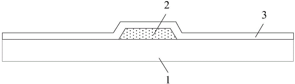
[0074] Step 1: Deposit a molybdenum / aluminum / molybdenum three-layer metal film on the base substrate 1 as a gate metal film, and the thickness of the molybdenum / aluminum / molybdenum three-layer metal film is 25 / / 100 / 25 nanometers respectively , the gate metal film is formed into the gate electrode 2 through a patterning process. Substrate substrate 1 is S with a thickness of 200 nanometers i o 2 The buffer layer is an alkali-free glass substrate. The schematic diagram after preparing the gate electrode 2 on the base substrate 1 is as follows figure 2 shown.

[0075] In step 2, a gate insulating layer 3 is deposited on the base substrate 1 after the above steps by using a plasma-enhanced chemical vapor deposition method. The schematic diagram after the gate insulating layer 3 is prepared is as follows: image 3 shown.

[0076] The...

Embodiment 2

[0087] The embodiment of the present invention provides a second specific method for preparing a metal oxide thin film transistor, including:

[0088] Step 1: On the base substrate 1, a copper metal film is deposited as a gate metal film by physical vapor deposition. The thickness of the copper metal film is 500 nanometers, and the gate metal film is formed into a gate electrode 2 through a patterning process. The base substrate 1 is Al with a thickness of 50 nanometers 2 o 3Flexible substrate for water and oxygen barrier layer. The schematic diagram after preparing the gate electrode 2 on the base substrate 1 is as follows figure 2 shown.

[0089] In step 2, a gate insulating layer 3 is deposited on the base substrate 1 after the above steps by using a plasma-enhanced chemical vapor deposition method. The schematic diagram after the gate insulating layer 3 is prepared is as follows: image 3 shown.

[0090] The gate insulating layer 3 is formed by stacking aluminum oxi...


PUM

PropertyMeasurementUnit
thicknessaaaaaaaaaa
thicknessaaaaaaaaaa
thicknessaaaaaaaaaa

Abstract

The invention discloses a film transistor and a preparation method thereof, an array substrate and a display panel, thus solving the problem of easy corrosion of the active layer when using back channel etching technology to make a metal oxide film transistor; the method comprises the following steps: forming a grid electrode metal film on a substrate, using a composition technology to form a grid electrode metal layer having a grid electrode on the grid electrode metal film; forming a grid electrode insulation layer on the grid electrode metal layer; forming the active layer on the grid electrode insulation layer; forming a metal nanometer particle layer on the active layer so as to serve as an etching protection layer; forming a source drain electrode metal film on the substrate finishing the said steps, using the composition technology to form a source drain electrode metal layer having a source electrode and a drain electrode on the source drain electrode metal film, and the source electrode and the drain electrode cover partial metal nanometer particle layer; using oxygen plasma to remove or oxidize a part, uncovered by the source electrode and drain electrode, of the metal nanometer particle layer; forming a passivation layer on the source drain electrode metal layer.

Description

technical field [0001] The present invention relates to the technical field of semiconductors, in particular to a thin film transistor and a preparation method thereof, an array substrate and a display panel. Background technique [0002] Flat panel displays (F1at Pane1Disp1ay, FPD) have become mainstream products on the market, and there are more and more types of flat panel displays, such as liquid crystal displays (Liquid CrystalDisp1ay, LCD), organic light emitting diodes (Organic Light Emitted Diode, OLED) displays, plasma Body display panel (P1asma Display Panel, PDP) and field emission display (Field Emission Display, FED), etc. [0003] The thin film transistor (Thin Film Transistor, TFT) backplane technology, which is the core technology of the FPD industry, is also undergoing profound changes. Especially the metal oxide thin film transistor (Metal Oxide Thin Film Transistor, MOTFT), due to its high mobility (about 5-50cm2 / Vs), simple manufacturing process, low cos...

Claims


Application Information

Patent Timeline
Patent Type & Authority Applications(China)
IPC IPC(8): H01L21/34H01L29/786
CPCH01L29/66969H01L29/7869H01L29/45H01L21/34B82Y30/00C09D11/52C23C14/086C23C14/14C23C14/223C23C14/5806C23C14/5853C23C14/5873C23C16/06C23C16/56C23C18/08C23C18/1254C23C18/1258C23C18/127C23C20/04C23C30/00H01L21/02118H01L21/02164H01L21/0217H01L21/02178H01L21/02183H01L21/02192H01L21/02274H01L21/02565H01L21/02631H01L21/288H01L21/443H01L21/445H01L21/47H01L21/473H01L21/47635H01L29/41733H01L29/42384H01L29/4908H01L29/78603H01L29/78696
Inventor 袁广才闫梁臣徐晓光王磊彭俊彪兰林锋
Owner BOE TECH GRP CO LTD
Why Eureka
Try Eureka