Thin film transistor and manufacturing method thereof

A technology of thin film transistor and manufacturing method, applied in transistor, semiconductor/solid-state device manufacturing, semiconductor device and other directions, can solve the problem of oxide semiconductor cutting and the like

Pending Publication Date: 2021-06-08
KUSN INFOVISION OPTOELECTRONICS +1
View PDF0 Cites 0 Cited by
  • Summary
  • Abstract
  • Description
  • Claims
  • Application Information

AI Technical Summary

Problems solved by technology

[0005] In order to solve the above technical problems, the present invention proposes a thin film transistor and its manufacturing method, which can well protect the oxide semiconductor from being etched by the etching solution, and solve the problem that the oxide semiconductor at the channel is cut off

Method used


Image

  • Thin film transistor and manufacturing method thereof
  • Thin film transistor and manufacturing method thereof
  • Thin film transistor and manufacturing method thereof

Examples


Embodiment Construction

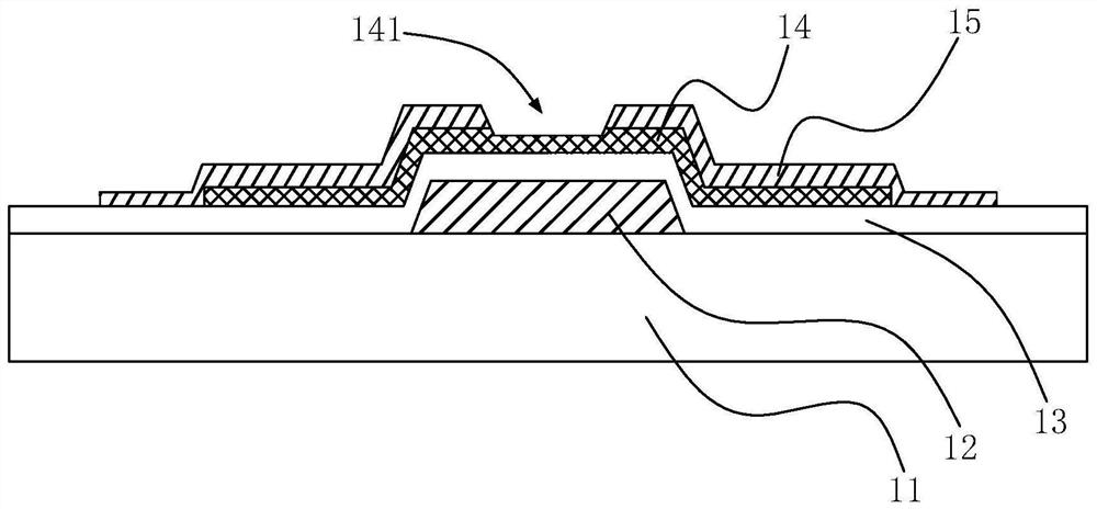
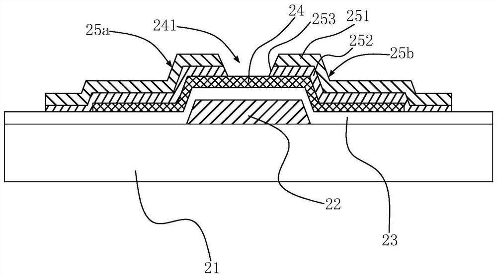
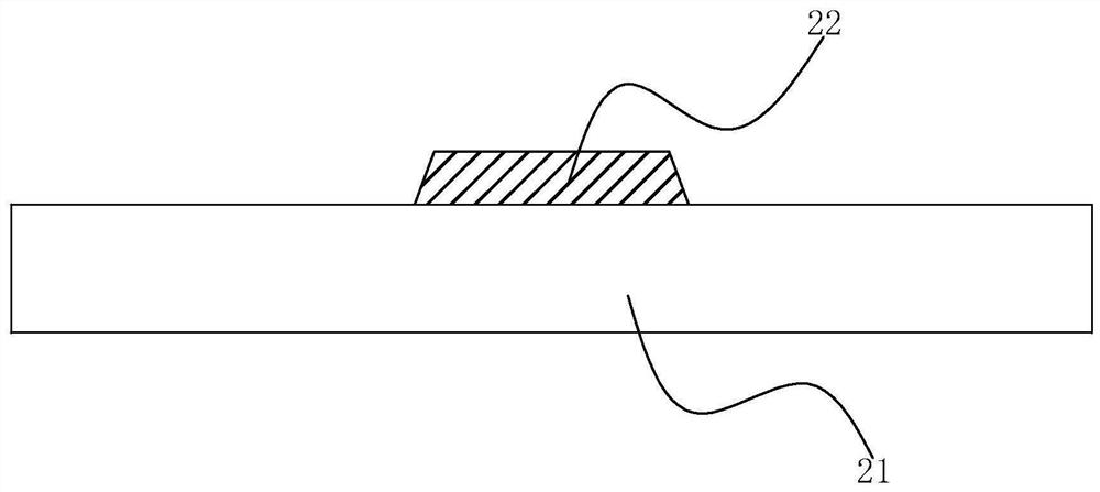
[0033] The specific implementation manners of the present invention will be further described in detail below in conjunction with the accompanying drawings and embodiments. The following examples are used to illustrate the present invention, but are not intended to limit the scope of the present invention.

[0034] Thin Film Transistor TFT (Thin Film Transistor) is widely used in display devices, and thin film transistor technology has also developed from the original a-Si (amorphous silicon) thin film transistor to the current LTPS (low temperature polysilicon) thin film transistor, oxide (oxide) thin film Transistors, etc. Among them, thin film transistors, which are compound semiconductor active layer materials represented by metal oxides, are more popular with the public because of their advantages such as high mobility, simple manufacturing process, good uniformity in large areas, and low manufacturing costs.

[0035] The invention provides a method for manufacturing a th...


PUM

PropertyMeasurementUnit
thicknessaaaaaaaaaa
thicknessaaaaaaaaaa
thicknessaaaaaaaaaa

Abstract

The invention provides a thin film transistor and a manufacturing method thereof, and the method comprises the following steps: providing a substrate, and forming a gate electrode on the substrate; depositing a gate electrode insulating layer covering the gate electrode on the substrate; forming an oxide semiconductor layer on the gate electrode insulating layer; continuously depositing a second metal layer and a first metal layer on the oxide semiconductor layer; coating a photoresist on the first metal layer; carrying out first wet etching on the exposed first metal layer by adopting first etching liquid; performing second wet etching on the exposed second metal layer by using a second etching solution; and removing the photoresist. According to the thin film transistor and the manufacturing method thereof provided by the invention, the oxide semiconductor layer can be well protected from being etched by etching liquid, and the problem that the oxide semiconductor layer at the channel is etched off is solved.

Description

technical field [0001] The invention relates to the display field, in particular to a thin film transistor and a manufacturing method thereof. Background technique [0002] With the continuous development of science and technology, the display technology has also developed rapidly. The thin film transistor TFT (Thin Film Transistor) technology has developed from the original a-Si (amorphous silicon) thin film transistor to the current LTPS (low temperature polysilicon) thin film transistor, Oxide (Oxide) thin film transistors, etc., thin film transistors of compound semiconductor active layer materials represented by metal oxides have the advantages of high mobility, simple manufacturing process, good large-area uniformity, and low manufacturing cost. [0003] In the manufacturing technology of oxide thin film transistors, the bottom gate back channel etching (Back Channel Etch, BCE) process and the etching stopper (Etch Stopper Type, ESL) process are usually used. The ESL p...

Claims


Application Information

Patent Timeline
Patent Type & Authority Applications(China)
IPC IPC(8): H01L21/44H01L21/34H01L29/417H01L29/786
CPCH01L29/401H01L29/41733H01L29/66969H01L29/7869
Inventor 章雯董承远
Owner KUSN INFOVISION OPTOELECTRONICS
Why Eureka
Try Eureka