Power semiconductor device type selection method

A power semiconductor and device technology, applied in the field of power semiconductor device evaluation, can solve problems such as inability to accurately judge the performance of power semiconductor devices, and achieve the effects of prolonging life and reducing the impact of output capabilities

Pending Publication Date: 2021-06-11
LEADRIVE TECH (SHANGHAI) CO LTD
View PDF10 Cites 0 Cited by
  • Summary
  • Abstract
  • Description
  • Claims
  • Application Information

AI Technical Summary

Problems solved by technology

[0004] In view of this, the present application provides a type selection method for power semiconductor devices, which solves the problem in the prior art that the performance of power semiconductor devices cannot be accurately judged for specific working conditions, and reduces the short-term impact of power semiconductor devices on the overall product. Effect of output capability, prolonging the lifetime of power semiconductor devices

Method used


Image

  • Power semiconductor device type selection method
  • Power semiconductor device type selection method
  • Power semiconductor device type selection method

Examples


Embodiment 1

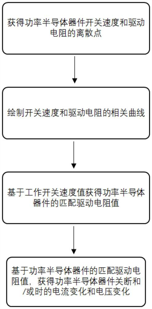
[0034] Such as figure 1 As shown, a power semiconductor device selection method includes the following steps:

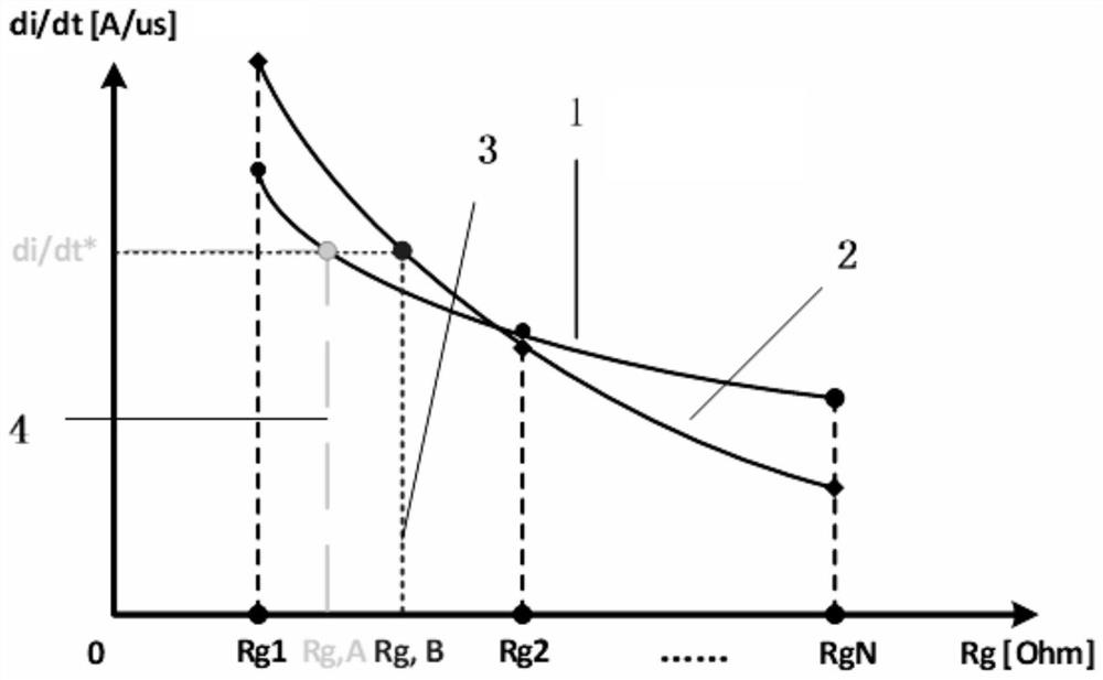
[0035] Step 1: Establish a Cartesian coordinate system, with the driving resistance as the abscissa and the switching speed as the ordinate. Under the same test environment and voltage, current and temperature settings, calibrate the corresponding switching speed of multiple power semiconductor devices under different driving resistance values, which is the calibrated switching speed value, and the calibrated switching speed value is the maximum value of the current change rate (di / dt , max), to get the discrete points of current change rate and drive resistance. In this embodiment, two power semiconductor devices are calibrated, and the two power semiconductor devices are A and B respectively. In other embodiments, three or four equal numbers of power semiconductor devices may also be calibrated. The calibrated switching speed value can also be the average value ...

Embodiment 2

[0045] A type selection method for a power semiconductor device, comprising the steps of:

[0046] Step 1: Establish a Cartesian coordinate system, with the driving resistance as the abscissa and the switching speed as the ordinate. Under the same test environment and voltage, current and temperature settings, calibrate the corresponding switching speed of a power semiconductor device under different driving resistance values, and obtain the discrete points of switching speed and driving resistance. In this embodiment, the switching speed is selected from the switching speed of the power semiconductor device rate of change of current.

[0047] In step 2, based on the discrete points of the power semiconductor device, a correlation curve between the current change rate and the driving resistance of the power semiconductor device is drawn by an interpolation method.

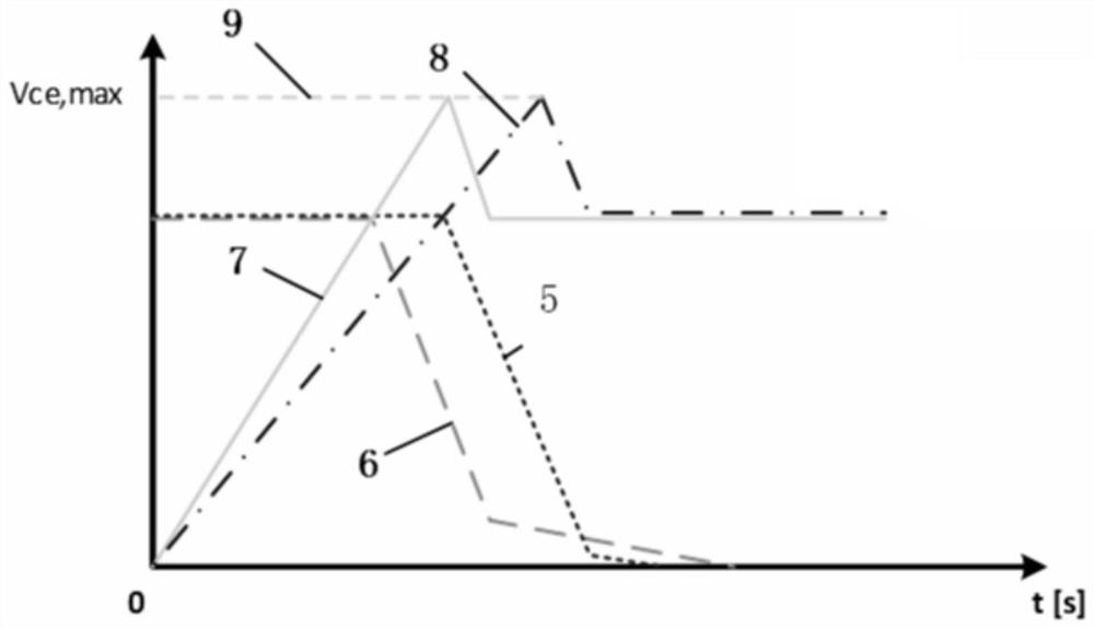
[0048] Step 3, then take the working current change rate value suitable for the actual working conditions as a ...


PUM


Abstract

The embodiment of the invention provides a power semiconductor device type selection method, which belongs to the technical field of power semiconductor device evaluation, and comprises the following steps: 1, obtaining the switching speed of a power semiconductor device and discrete points of a driving resistor; 2, obtaining a correlation curve of the switching speed and the driving resistance; 3, obtaining a working switching speed value based on the requirement of an actual working condition, and obtaining a matched driving resistance value corresponding to the working switching speed value of the power semiconductor; and 4, obtaining current change and voltage change when the power semiconductor device is turned off and/or turned on based on the power semiconductor device under the configuration matching driving resistance value, and judging the performance of the power semiconductor device. Through the processing scheme provided by the invention, the problem that the performance of the power semiconductor device cannot be accurately judged under a specific working condition in the prior art is solved.

Description

technical field [0001] The present application relates to the technical field of power semiconductor device evaluation, in particular to a method for selecting a power semiconductor device. Background technique [0002] Power semiconductor devices are the core of equipment such as frequency conversion / rectification / inverter in the power electronics industry, and determine the key electrical performance of the system. Therefore, screening out power semiconductor devices with excellent performance and suitable for applications is an important step in device evaluation, drive design and system design. [0003] Most of the current evaluation methods for power semiconductor devices mainly refer to the data sheets of the devices, so that simple test applications can be carried out to meet the needs. However, the data in the data sheets of various power semiconductor device manufacturers and the working conditions in the application are different, so it is difficult to use them as...

Claims


Application Information

Patent Timeline
Patent Type & Authority Applications(China)
IPC IPC(8): G01R31/26
CPCG01R31/2603
Inventor 夏雨昕沈捷林昆鹏
Owner LEADRIVE TECH (SHANGHAI) CO LTD
Why Eureka
Try Eureka