Touch drive circuit, drive chip and touch display device
A technology of touch drive circuit and touch electrode, which is applied in the direction of electrical digital data processing, instrumentation, data processing input/output process, etc., and can solve problems such as difficulty in meeting low-power touch detection and increased power consumption of OLED screens
Active Publication Date: 2021-06-11
SHENZHEN GOODIX TECH CO LTD
5 Cites 0 Cited by
AI-Extracted Technical Summary
Problems solved by technology
However, compared to LCD screens, the load capacitance of OLED screens (equivalent capacitance C L ) The capacitance value is significantly larg...
Method used
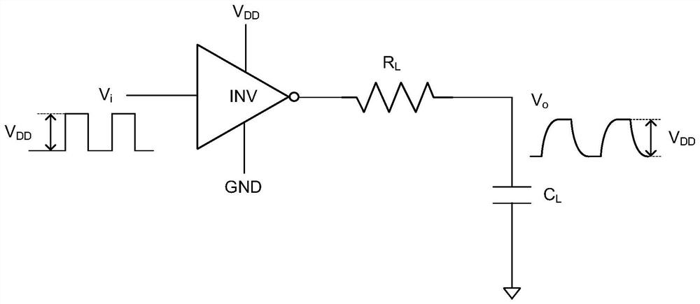
[0043] By setting the first negative voltage -VDD, the signal amplitude of the driving signal output by the touch driving circuit can be increased from VDD to 2VDD, which is beneficial to improve the resolution of touch detection. For the traditional touch driving circuit shown in Figure 1, if the signal amplitude of the driving signal increases to 2VDD, the driving power consumption in one period T will increase to 4*CL*VDD2*f; The loss on resistor RL is equal to 2*CL*VDD2*f. However, in this embodiment, the first energy storage capacitor CS1 and the second energy storage capacitor CS2 are used to recycle the charges transferred from the touch electrodes during the discharge process, and no additional power consumption will be generated during this process. Therefore, during the discharge process of the touch electrodes, the loss on the resistor RL is equal to 1/2*CL*VDD2*f, which is only 25% of the traditional touch driving circuit.
[0091] It should be noted that the touch drive circuit provided in the embodiment of the present application can not only use two energy storage capacitors, but also four or more paired energy storage capacitors, each pair of energy storage capacitors respectively It is used to provide positive and n...
Abstract
The invention provides a touch drive circuit, a drive chip and a touch display device. The touch drive circuit is used for outputting a driving signal to drive a touch electrode of the touch display device. The touch drive circuit comprises a power supply voltage generating circuit, a switching circuit and a first energy storage capacitor, the first input end of the switching circuit is connected to the power supply voltage generating circuit; a second input end of the switching circuit is connected to a ground end GND through a first energy storage capacitor; a third input end of the switching circuit is connected to a ground end GND; the output end of the switching circuit is connected to the touch electrode; the power voltage generation circuit is used for generating first positive voltage; and the switching circuit is used for controlling the touch electrode to be connected to the power supply voltage generating circuit in a first time period, controlling the touch electrode to be connected to the first energy storage capacitor in a second time period and controlling the touch electrode to be connected to a ground end GND in a third time period. The touch drive circuit has relatively low driving power consumption.
Application Domain
Input/output processes for data processing
Technology Topic
CapacitanceHemt circuits +7
Image
Examples
- Experimental program(1)
Example Embodiment
[0031] The technical solutions in the present application embodiment will be described below in conjunction with the accompanying drawings, as will be described, and the described embodiments are part of the embodiments of the present application, not all of the embodiments.
[0032] The term used herein is to describe the embodiments of the particular embodiment, not intended to limit the application. "One", "one", "one", "one", "" "," and "" "as used in the present application and the appended claims are also intended to include many forms unless otherwise clearly indicated. It should also be understood that the terms "and / or" as used herein refer to any or from any or more of the associated listing items.
[0033] In addition, the terms such as "first", "second" are only used to distinguish the similar objects, and cannot be understood as an indication or implicit relative importance, or implicitly indicated the number of technical features indicated. Thereby, features with "first", "second", and the like may be indicated or implicitly including one or more of this feature.
[0034] The present application provides a touch drive circuit, a drive chip, and a touch display device. The touch drive circuit can be applied to the touch display device, and the output drive signal is output to drive the touch electrode of the touch display device. The touch display device can also include a display, and the user can utilize a finger or other conductor touch the corresponding touch operation; examples of the display include, but are not limited to, liquid crystal (LCD) displays, organic light emitting (OLED) Display, plasma (PDP) displays, and cathode rays (CRT) displays.
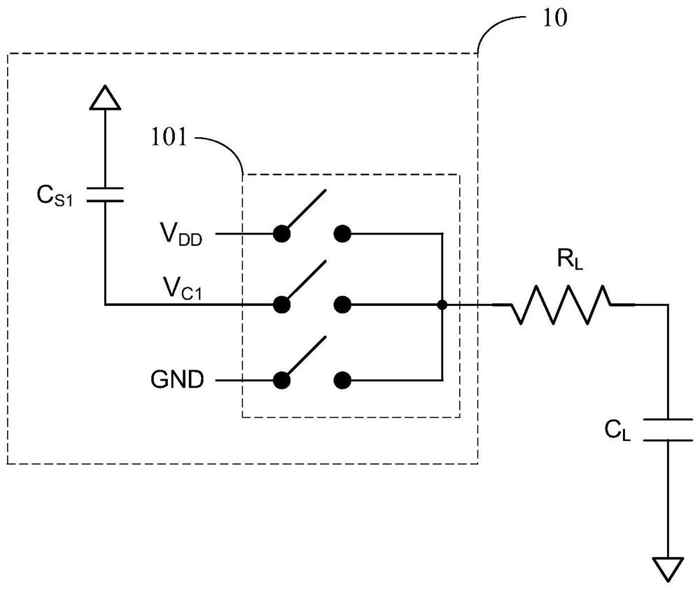
[0035] Such as figure 2 As shown, a configuration diagram of a touch driving circuit is provided for the embodiment of the present application embodiment. Among them, the resistance R L Indicates the drive impedance (including the equivalent impedance of the touch electrode and the touch drive circuit); capacitor C L Indicates the equivalent capacitance of the touch electrode. The touch drive circuit 10 includes a switching circuit 101, and the first input end of the switching circuit 101 is connected to the first positive voltage V. DD The second input is passed through the first storage capacitor C. S1 Connect to the ground GND, the third input is connected to the ground GND, and the output is connected to the touch electrode. First positive voltage V DD The power supply voltage generated by the power supply voltage generated circuit can be used. The switching circuit 101 can control the connection object of the touch electrode in order to control the touch electrode in the first time period, the control of the touch electrode is connected to the power supply voltage generating circuit, and the first positive voltage is charged to the touch electrode, so that the voltage across the touch electrode Equal to the first positive voltage V DD; Control the touch electrode in the second time period to the first storage capacitor C S1 , First storage capacitor C S1 The charge of the touch electrode can be stored such that the voltage across the touch electrode is equal to the second positive voltage V. C1 And in the third time, the control of the touch electrode is connected to the ground GND, the touch electrode is discharged, so that the voltage at both ends of the touch electrode is equal to the zero voltage.
[0036] Wherein, the power supply voltage generating circuit may be provided to provide a power supply voltage to the touch drive circuit, or may be shared with other circuit modules in the touch detection chip.
[0037] Since the touch electrode towards the first storage capacitor C S1 Transferring a portion of the positive charge, until the voltage at both ends of the touch electrode and the first storage capacitor C S1 The voltage equal to both ends such that the voltage at both ends of the touch electrode is from the first positive voltage V DD Changed to the second positive voltage V C1 , So the second positive voltage V C1 Lower than the first positive voltage V DD And above zero voltage, that is, satisfying V DD V C1 0.
[0038] When the first storage capacitor C S1 The capacitance value is much larger than the capacitor C. L When the capacitance value is values, the second positive voltage V C1 Approximate equal to V DD / 2,, in the discharge process of the touch electrode, the resistance R L Above the loss is approximately equal to 1/4 * C L * V DD 2 * f, only figure 1 50% of the conventional touch drive circuit shown, in particular, if the first storage capacitor C S1 The capacitance value is greater than the capacitor C. L 30 times the capacitance value, it can be determined that the first storage capacitor C S1 The capacitance value is much larger than the capacitor C. L The capacitance value; preferably, the first storage capacitor can S1 The capacitance value is greater than the capacitor C. L 50 to 100 times the capacitance value.
[0039] In addition, when the first storage capacitor C S1 The capacitance value is not much larger than the capacitor C. L When the capacitance value, the first storage capacitor C is S1 Can also introduce a lower than the first positive voltage V DD And higher than the intermediate level of the zero voltage, thereby reducing the resistance R during discharge of the touch electrode L The loss can make the loss value of less than 1/2 * c L * V DD 2 * f, but because the intermediate level is not approximately equal to V DD / 2, so it will result in this loss value greater than 1/4 * c L * V DD 2 * f.
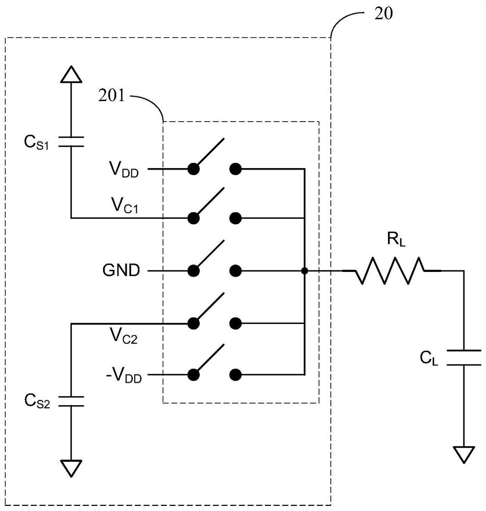
[0040] Such as image 3 As shown, the structure is shown in another touch driving circuit provided in the present application embodiment. The touch drive circuit 20 includes a switching circuit 201, and the first input terminal of the switch circuit 201 is connected to the first positive voltage V. DD The second input is passed through the first storage capacitor C. S1 Connect to the ground GND, the third input is connected to the ground GND, the fourth input is passed through the second storage capacitor C. S2 Connect to the ground GND, the fifth input is connected to the first negative voltage -V DD The output is connected to the touch electrode. First positive voltage V DD And the first negative voltage -V DD Both are the power supply voltages generated by the power supply voltage generating circuit. The switching circuit 201 can control the connection object of the touch electrode in order, in the following order, control the touch electrode connected to the power supply voltage generating circuit, and the first positive voltage is charged to the touch electrode, so that the voltage across the electrode Equal to the first positive voltage V DD; Control the touch electrode in the second time period to the first storage capacitor C S1 , First storage capacitor C S1 The charge of the touch electrode can be stored such that the voltage across the touch electrode is equal to the second positive voltage V. C1 In the third time, the control of the touch electrode is connected to the ground GND, and the touch electrode is discharged, so that the voltage across the touch electrode is equal to the zero voltage; control the touch electrode to the second storage capacitor C in the fourth time period. S2 , Second storage capacitor C S2 Transferring the stored charge to the touch electrode so that the voltage across the touch electrode is equal to the second negative voltage V C2 Control the touch electrode to access the first negative voltage -V in the fifth time period DD , First negative voltage -V DD The touch electrode is charged such that the voltage across the touch electrode is equal to the first negative voltage -V DD.
[0041] Among them, the power supply voltage generating circuit can include a positive and negative voltage conversion circuit, and the positive and negative voltage conversion circuit can put the first positive voltage V. DD Convert to the first negative voltage -V DD Examples of the positive and negative voltage conversion circuit include a negative pressure charge pump circuit.
[0042] The charge transfer process in the fourth time period is based on the second storage capacitor C. S2 A certain negative charge has been stored. Due to the first negative voltage -V due to the fifth time period DD Further, the touch electrode is charged such that the voltage across the touch electrode is from the second negative voltage V. C2 Changed to the first negative voltage -V DD , So the second negative voltage V C2 Above first negative voltage -V DD , And below zero voltage, satisfying 0> V C2 -V DD , │V DD │> │V C2 │> 0.
[0043] By setting the first negative voltage -V DD , Can cause the signal of the drive signal output from the touch drive circuit from V DD Rising to 2VDD It is conducive to improving the resolution of touch detection. for figure 1 The conventional touch drive circuit shown, if the signal amplitude of the drive signal is increased to 2V DD , The driving power consumption in one cycle T will increase to 4 * c L * V DD 2 * f; wherein the resistance R in the touch electrode discharge process L The loss is equal to 2 * C L * V DD 2 * f. However, in the present embodiment, the first storage capacitor C is utilized. S1 And the second storage capacitor C S2 The recycled charge is transferred by the touch electrode during the discharge process, and no additional power consumption is generated during this process, so that the resistance R in the discharge process of the touch electrode L The loss is equal to 1/2 * C L * V DD 2 * f, only 25% of the traditional touch drive circuit.
[0044] Based on the above embodiment disclosed, in the present embodiment, the switching circuit can further control the touch electrode to the second storage capacitor C within the sixth time period. S2 , Second storage capacitor C S2 The charge of the touch electrode is released, so that the voltage across the touch electrode is equal to the second negative voltage V C2 In the seventh time, the control of the touch electrode is connected to the ground GND, and the touch electrode is discharged, so that the voltage across the touch electrode is equal to the zero voltage; the control of the touch electrode is connected to the first storage capacitor C in the eighth time period. S1 , First storage capacitor C S1 Transferring the stored charge to the touch electrode such that the voltage across the touch electrode is equal to the second positive voltage V C1. At this point, the switching circuit completes the operation within a working cycle, and next, according to the operation within the first time period, control the first positive voltage V. DD Charging the touch electrode and continues to periodically cycle, so that the signal amplitude of the drive signal output from the touch drive circuit is equal to the first positive voltage, the second positive voltage, zero voltage, and the second negative voltage, The first negative voltage, the second negative voltage, zero voltage, and the second positive voltage.
[0045] When the touch drive circuit is in the initial state, the first storage capacitor C S1 And the second storage capacitor C S2 The amount of charge of the stored charge is zero, which can cause the switch circuit to sequentially control: the first positive voltage V in accordance with the first time period to the eighth time period. DD Charging the touch electrode until the voltage at both ends of the touch electrode is equal to the first positive voltage V DD; Touch electrode and the first storage capacitor C S1 Connected, and to the first storage capacitor C S1 Transfer a portion of the positive charge until the voltage across the touch electrode is equal to the second positive voltage V C1 The touch electrode is grounded and discharged, until the voltage across the touch electrode is equal to 0; the touch electrode and the second storage capacitor C S2 Connected, but due to the second storage capacitor C S2 The amount of charge is 0, so the touch electrode and the second storage capacitor C. S2 No charge transfer occurs; first negative voltage -V DD Charge the touch electrode until the voltage at both ends of the touch electrode is equal to the first negative voltage -V DD; Touch electrode again with the second storage capacitor C S2 Connected, and touch the electrode to the second storage capacitor C S2 Discharge, second storage capacitor C S2 The charge of the touch electrode is stored until the voltage at both ends of the touch electrode is equal to the second negative voltage V C2 The touch electrode is again grounded and discharged, until the voltage at both ends of the touch electrode is equal to 0; the touch electrode and the first storage capacitor C S1 Connected, the first storage capacitor C S1 Transferring the stored charge to the touch electrode, charging the touch electrode until the voltage at both ends of the touch electrode is equal to the second positive voltage V C1 Next, periodically cycle the above process, when the touch electrode is switched from the ground to the second storage capacitor C S2 When the second storage capacitor C S2 The stored charge can be transferred to the touch electrode to charge the touch electrode until the voltage across the touch electrode is equal to the second negative voltage V. C2. Thereby, the first storage capacitor C S1 And the second storage capacitor C S2 The amount of charge of the stored charge can be gradually stable, so that the second positive voltage V is C1 And the second negative voltage V C2 The value gradually stabilizes, and when the first storage capacitor C S1 And the second storage capacitor C S2 The capacitance value is much larger than the capacitor C. L When the capacitance value is in the with capacitor C L The first storage capacitor C before and after charging transfer S1 And the second storage capacitor C S2 The amount of charge stored hardly changes.
[0046] Based on the above embodiment, in this embodiment, the switching circuit may further include a first switching circuit, a second switching circuit, a third switching circuit, a fourth switching circuit, and a fifth switching circuit. Specifically, the input of the first switch circuit is the first input of the switching circuit, the output of the first switch circuit is connected to the output of the switch circuit; the input end of the second switch circuit is the second input of the switching circuit, The output of the second switch circuit is connected to the output of the switch circuit; the input end of the third switch circuit is the third input of the switch circuit, the output of the third switching circuit is connected to the output of the switching circuit; the fourth switching circuit The input terminal is the fourth input of the switch circuit, the output of the fourth switch circuit is connected to the output of the switch circuit; the input end of the fifth switch circuit is the fifth input of the switch circuit, the output of the fifth switching circuit. Connect to the output of the switching circuit.
[0047] When any of the above-mentioned switching circuits, the other four switching circuits remain open, i.e., at a single moment, only one switching circuit is turned on. In this embodiment, the five switching circuits may periodically circulate in accordance with the following order:
[0048] In the first time period, only the first switch circuit is turned on, the first positive voltage V DD The touch electrode is charged such that the voltage across the touch electrode is equal to the first positive voltage V DD. During the second time, only the second switching circuit is turned on, the touch electrode is connected to the first storage capacitor C S1 , First storage capacitor C S1 The charge of the touch electrode is stored such that the voltage across the touch electrode is equal to the second positive voltage V C1 In the third time, only the third switching circuit is turned on, the touch electrode is connected to the ground GND, the touch electrode is discharged, so that the voltage across the touch electrode is equal to zero voltage; in the fourth time period, only the fourth switch only Circuit is turned on, the touch electrode is connected to the second storage capacitor C S2 , Second storage capacitor C S2 Transferring the stored charge to the touch electrode so that the voltage across the touch electrode is equal to the second negative voltage V C2 In the fifth time period, only the fifth switching circuit is turned on, the touch electrode is connected to the first negative voltage -V DD , First negative voltage -V DD The touch electrode is charged such that the voltage across the touch electrode is equal to the first negative voltage -V DD In the sixth time period, only the fourth switching circuit is turned on, the touch electrode is connected to the second storage capacitor C. S2 , Second storage capacitor C S2 The charge of the touch electrode is released, so that the voltage across the touch electrode is equal to the second negative voltage V C2 In the seventh time, only the third switch circuit is turned on, the touch electrode is connected to the ground GND, the touch electrode is discharged, so that the voltage across the touch electrode is equal to zero voltage; in the eighth time period, touch electrode Connect to the first storage capacitor C S1 , First storage capacitor C S1 Transferring the stored charge to the touch electrode such that the voltage across the touch electrode is equal to the second positive voltage V C1.
[0049] Further, since the voltage at both ends of the touch electrode often needs to achieve a stable value, in order to ensure that the touch electrodes can be sufficiently charged in the corresponding period, it can be set A switching circuit, a second switching circuit, a third switching circuit, a fourth switching circuit, and a stepping time of the fifth switching circuit are greater than or equal to the time of the voltage of the electrodes to establish to the stable value within the corresponding period, thereby ensuring touch The signal amplitude of the drive signal output of the drive circuit and the driving power consumption of the touch drive circuit can achieve the target value of the design. For example, in the first time period, the first switching circuit is turned on, and the touch driving circuit outputs the first positive voltage to charge the electrode, and when the voltage in the electrode is raised to the stabilizing value, or in the electrode. After the voltage is raised to the stability value, the first switch circuit is turned on, and the second switching circuit is turned on; if the voltage is not raised to the stabilization value, the second switch is turned off, and the second switch is disconnected. The circuit is turned on, which causes the positive voltage amplitude of the drive signal to reach V. DD Further, the signal amplitude of the drive signal cannot reach 2V. DD Further, for example, in the fourth time period, the fourth switching circuit is turned on, and the voltage at both ends of the touch electrode begins by the zero voltage. If the voltage at both ends of the touch electrode does not fall to the stabilizing value, the fourth switch will The circuit is disconnected, and the fifth switching circuit is turned on, i.e., the power supply voltage generating circuit is driven to drive the touch electrode, and the voltage variation of the touch electrode at both ends of the touch electrode is directly driven by the power supply voltage on the touch electrode directly by the power supply voltage. Increased, thereby causing greater driving power consumption.
[0050] Such as Figure 4 As shown, a waveform of a driving signal provided in the present application embodiment, the drive signal can be image 3 The touch drive circuit shown, and the second positive voltage V C1 And the second negative voltage V C2 The value has been basically stable. It can be seen that the waveform of the drive signal is stepped, the signal amplitude is 2V. DD And in one cycle T, only the first time period And fifth time Directly charge the touch electrode directly by the power supply voltage, which is equivalent to only the first time period And fifth time Generate actual drive power consumption. Due to the operation of the touch drive circuit, the first storage capacitor C S1 Equivalent capacitance C with touch electrode C L There is a charge transfer, so before and after the charge transfer, the first storage capacitor C S1 The amount of charge and the voltage value at both ends have a certain change, in order to facilitate the calculation of the driving power consumption of the touch drive circuit, the first time period Internal first storage capacitor C S1 The voltage at both ends tends to stabilize the value of V. C1_1 , The second time period Internal first storage capacitor C S1 The voltage at both ends tends to stabilize the value of V. C1_2.
[0051] Such as Figure 5 As shown, a first time period provided by the embodiment of the present application And the second time The internal touch drive circuit is schematically illustrated on the touch electrode; the first storage capacitor C S1 The voltage value on both ends has been basically stable. It can be seen, in the first time period Internal, first positive voltage V DD Equivalent capacitor C for touch electrode C L Charging, first storage capacitor C S1 The voltage stabilized at both ends in the voltage value V C1_1 In the second time period Equivalent capacitance C in touch electrode L To the first storage capacitor C S1 Transfer positive charge to make the equivalent capacitor C L And the first storage capacitor C S1 The voltage at both ends is stable in the voltage value V C1_2 And voltage value V C1_2 Slightly above the voltage value V C1_1. According to the law of charge conservation, the above respective voltage values and capacitance values are satisfied:
[0052] V DD * C L + V C1_1 * C S1 = V C1_2 * (C L + C S1 ) (Formula 1)
[0053] Such as Figure 6 As shown, a seventh time period provided in the present application embodiment And eighth time The internal touch drive circuit is schematically illustrated on the touch electrode. Can be seen, in the seventh time Equivalent capacitance C in touch electrode L Discharge, first storage capacitor C S1 The voltage stabilized at both ends in the voltage value V C1_2 In the eighth time Equivalent capacitance C in touch electrode L To the first storage capacitor C S1 Transfer negative charge to make the equivalent capacitor C L And the first storage capacitor C S1 The voltage at both ends is stable in the voltage value V C1_1. According to the law of charge conservation, the above voltage value and the capacitance value satisfy the following relationship:
[0054] V C1_2 * C S1 = V C1_1 * (C L + C S1 (Equation 2)
[0055] Combined with Equation 1 and Equation 2, it can be calculated:
[0056] V C1_1 = V DD * C S1 / (2C S1 + C L (Equation 3)
[0057] V C1_2 = V DD * (C L + C S1 ) / (2C S1 + C L (Equation 4)
[0058] When the first storage capacitor C S1 The capacitance value is much larger than the capacitor C. L Capacitor value (ie C S1 C L When you can get: V C1_1 ≈V C1_2 ≈1 / 2V DD. Specifically, it can be in the first storage capacitor C S1 The capacitance value is greater than the capacitor C. L When 50 to 100 times the capacitance value, determine the first storage capacitor C S1 The capacitance value is much larger than the capacitor C. L The capacitance value.
[0059] Similarly, when the second storage capacitor C S2 The capacitance value is much larger than the capacitor C. L When the capacitance value, the second negative voltage V can be obtained. C2 Approximate equal to -1 / 2V DD. Specifically, can be in the second storage capacitor C S2 The capacitance value is greater than the capacitor C. L When 50 to 100 times the capacitance value, the second storage capacitor C is determined S2 The capacitance value is much larger than the capacitor C. L The capacitance value.
[0060] Due to only the first time during one cycle T And fifth time The touch electrode is driven directly from the power supply voltage, which is equivalent to generating the actual driving power consumption only in these two periods, so when the frequency of the drive signal is f, it can be calculated image 3 The actual drive power consumption shown in a cycle T actually drives P = (1 / 2V) DD ) * C L * f * v DD * 2 = C L * V DD 2 * f, and the signal amplitude of the drive signal is 2V DD Where f = 1 / t is the frequency of the drive signal. However, for a conventional touch drive circuit, when the output drive signal has a signal amplitude of 2V DD When the driving power consumption in one cycle T is 4 * c L * V DD 2 * f. Therefore, the touch driving circuit provided herein provides a high drive voltage while providing a high drive voltage.
[0061] It should be noted that the driving power consumption of the touch drive circuit can also be divided into two parts, one of which is the resistance R when charging the touch electrode L The upper loss, the other part is the resistance R when the touch electrode is discharged. L Lost, these two partial losses are 1/2 * c in one cycle T L * V DD 2 * f, the touch drive circuit is currently c contemporary in one cycle T L * V DD 2 * f.
[0062] Further, in the present application embodiment, the first storage capacitor C can be provided. S1 And the second storage capacitor C S2 The capacitance value is equal, and it is much larger than the equivalent capacitive value C of the touch electrode. L , Set C S1 = C S2 C L.
[0063] Specifically, the respective switching circuits in the present application embodiment may consist of one or more MOS (Metal-Oxide-Semiconductor, metal-oxide-semiconductor) field effect tubes, which are simply referred to as MOS tubes in order to facilitate description.
[0064] Such as Figure 7 As shown, it is a structural diagram of still another touch driving circuit according to the embodiment of the present application. Based on the above embodiment disclosed, in the present embodiment, the first switching circuit further includes a first MOS tube S. A1 The second switching circuit further includes a second MOS tube S A2 The fourth switching circuit further includes a fourth MOS tube S B1 The fifth switching circuit further includes a fifth MOS tube S B2 The third switching circuit further includes a third MOS tube S A3 And sixth MOS tube s B3; Where the first MOS pipe S A1 , Sixth MOS tube S B3 And the first pressure pipe S CA All are P-type MOS tubes, the second MOS pipe S A2 , Third MOS tube S A3 , Fourth MOS tube S B1 , Fifth MOS tube S B2 And the second pressure pipe S CB All are N-type MOS tubes.
[0065] Please refer to Figure 7 The specific connection relationship of each element in the touch driving circuit 30 is as follows: the first MOS tube S A1 Source Access First Positive Voltage V DD , First MOS pipe S A1 Open drain to the first pressure pipe S CA Source; second MOS tube S A2 Source connection to the first pressure pipe S CA Source, second MOS pipe S A2 Oil can be connected to the first storage capacitor C S1 The first end; the third MOS pipe S A3 Source connection to ground GND, third MOS tube S A3 Open drain to the first pressure pipe S CA Source; fourth MOS pipe S B1 Source connection to the second storage capacitor C S2 The first end, the fourth MOS pipe S B1 Object to the second pressure pipe S CB Source; fifth MOS pipe S B2 Source Access First Negative Voltage -V DD , Fifth MOS tube S B2 Object to the second pressure pipe S CB Source; sixth MOS tube S B3 Source connection to ground GND, sixth MOS pipe S B3 Object to the second pressure pipe S CB Source; first storage capacitor C S1 And the second storage capacitor C S2 The second end is connected to the ground GND; the first pressure pipe S CA And the second pressure pipe S CB The drain is both connected to the touch electrode.
[0066] Since the MOS tube element obtained by the CMOS process is usually equal to the power supply voltage V DD However, in part, the voltage values across several MOS tubes in the switching circuit exceed their resistance values, so it is easy to cause problems such as MOS tube burnout. Therefore, the first pressurizing tube S can be respectively according to the pressure difference between the respective MOS tubes at both ends of the respective MOS tubes. CA And the second pressure pipe S CB The gate access voltage is set to prevent the voltage from which the voltage at both ends of the MOS tube exceeds its voltage resistance, and does not affect the touch drive circuit to charge and discharge the touch electrode. Specifically, the first pressure pipe S CA Can prevent the first MOS tube S A1 , Second MOS tube S A2 And the third MOS tube S A3 The voltage over both ends exceeds its voltage resistance; the second pressure pipe S CB Can prevent the fourth MOS tube S B1 , Fifth MOS tube S B2 And sixth MOS tube s B3 The voltage at both ends exceeds its voltage resistance. Among them, the voltage across the MOS tube is specific to the voltage between the source and the drain of the MOS tube, that is, the source leakage voltage V. SD Or leak voltage V DS.
[0067]In this embodiment, in order to make the signal amplitude of the drive signal output from the touch driving circuit 30 in one cycle is equal to the first positive voltage, the second positive voltage, zero voltage, the second negative voltage, the first negative voltage, the second Negative voltage, zero voltage, second positive voltage, can control individual MOS tubes in the switching circuit, periodically circulate, and any of the MOS tubes in the switching circuit, other five MOS tubes remain Disconnect, that is, only one MOS tube is turned on in a single moment:
[0068] In the first time period, the first MOS tube S A1 Tong, the first pressure pipe S CA And the second pressure pipe S CB The gate is connected to the ground GND, and the other five MOS tube is turned off.
[0069] During this time period, since the first pressure pipe S CA Gate voltage V a Equal to 0, the source voltage is higher than the gate voltage V a , So the first pressure pipe S CA Tong, does not affect the touch drive circuit 30 output the first positive voltage V DD Capacitor C L Charging until capacitance C L The voltage at both ends is equal to the first positive voltage V DD. Also because the second pressure pipe S CB Gate voltage V b Equal to 0, so only when the second pressure pipe S CB When the source voltage is less than 0, the second pressure pipe S CB Can be turned on, while the second pressure pipe S CB When the source voltage is above or equal to 0, the second pressure pipe S CB As of this time, the second pressure pipe S is in this period. CB Defined, avoiding the fourth MOS tube S B1 , Fifth MOS tube S B2 And sixth MOS tube s B3 Leakage source voltage exceeds the voltage-specific value V DD Thereby prevent fourth MOS tube S B1 , Fifth MOS tube S B2 And sixth MOS tube s B3 Burnout.
[0070] In the second time period, the second MOS pipe S A2 Tong, the first pressure pipe S CA And the second pressure pipe S CB The gate is connected to the ground GND, and the other five MOS tube is turned off.
[0071] During this time period, since the first pressure pipe S CA Gate voltage V a Equal to 0, the source voltage is higher than the gate voltage V a , So the first pressure pipe S CA Tong, do not affect capacitive C L First storage capacitor C S1 Discharge until capacitance C L The voltage and the first storage capacitance at both ends C S1 Even if the voltage is equal to both ends L The voltage at both ends is made from the first positive voltage V DD Changed to the second positive voltage V C1 (0 C1 DD ). Also because the second pressure pipe S CB Gate voltage V b Equal to 0, so the second pressure pipe S CB Defined, avoiding the fourth MOS tube S B1 , Fifth MOS tube S B2 And sixth MOS tube s B3 Leakage source voltage exceeds the voltage-specific value V DD.
[0072] In the third time, the third MOS tube S A3 Tong, the first pressure pipe S CA The voltage value of the gate access is equal to the second positive voltage V C1 Minus the first positive voltage V DD Difference, ie the first pressure pipe S CA The voltage value of the gate access is equal to V C1 -V DD , Second pressure pipe S CB The gate is connected to the ground GND, and the other five MOS tube is turned off.
[0073] During this time period, since the first pressure pipe S CA Gate voltage V a Equal to V C1 -V DD , So the gate voltage V a <0, the source voltage is higher than the gate voltage V a , First pressure pipe S CA Tong, do not affect capacitive C L Discharge the capacitor C L The voltage at both ends is from the second positive voltage V C1 Change to 0. Also because the second pressure pipe S CB Gate voltage V b Equal to 0, so the second pressure pipe S CB Defined, avoiding the fourth MOS tube S B1 , Fifth MOS tube S B2 And sixth MOS tube s B3 Leakage source voltage exceeds the voltage-specific value V DD. In addition, when the first storage capacitor C S1 The capacitance value is much larger than the capacitor C. L When the capacitance value, V a = V C1 -V DD ≈-1 / 2V DD.
[0074] In the fourth time period, the fourth MOS tube S B1 Tong, the first pressure pipe S CA And the second pressure pipe S CB The gate is connected to the ground GND, and the other five MOS tube is turned off.
[0075] During this period, since the second pressure pipe S CB Gate voltage V b Equal to 0, the source voltage is less than the gate voltage V b , So the second pressure pipe S CB Tong, does not affect the second storage capacitor C S2 Capacitor C L Charging, making capacitor C L The voltage between the two ends and the second storage capacitor C S2 Even if the voltage is equal to both ends L The voltage at both ends is changed from 0 to the second negative voltage V C2 (V C2 <0). Also because the first pressure pipe S CA Gate voltage V a Equal to 0, so only when the first pressure pipe S CA When the source voltage is higher than 0, the first pressure pipe S CA Tong, while when the first pressure pipe S CA When the source voltage is less than or equal to 0, the first pressure pipe S CA The first pressure tube S is in this period CA As close, the first MOS pipe S can be avoided A1 , Second MOS tube S A2 And the third MOS tube S A3 The source leakage voltage exceeds the voltage-resistant value V DD.
[0076] In the fifth time period, the fifth MOS tube S B2 Tong, the first pressure pipe S CA And the second pressure pipe S CB The gate is connected to the ground GND, and the other five MOS tube is turned off.
[0077] During this period, since the second pressure pipe S CB Gate voltage V b Equal to 0, the source voltage is less than the gate voltage V b , So the second pressure pipe S CB Tong, does not affect the touch drive circuit 30 output the first negative voltage -V DD Capacitor C L Charging, making capacitor C L The voltage at both ends is from the second negative voltage V C2 Changed to the first negative voltage -V DD. Also because the first pressure pipe S CA Gate voltage V a Equal to 0, so the first pressure pipe S CA Definition, can avoid the first MOS tube S A1 , Second MOS tube S A2 And the third MOS tube S A3 The source leakage voltage exceeds the voltage-resistant value V DD.
[0078] In the sixth time period, the fourth MOS tube S B1 Tong, the first pressure pipe S CA And the second pressure pipe S CB The gate is connected to the ground GND, and the other five MOS tube is turned off.
[0079] During this stage, due to the second pressure pipe S CB Gate voltage V b Equal to 0, the source voltage is less than the gate voltage V b , So the second pressure pipe S CB Tong, do not affect capacitive C L Second storage capacitor C S2 Discharge until capacitance C L The voltage between the two ends and the second storage capacitor C S2 Even if the voltage is equal to both ends L The voltage at both ends is from the first negative voltage -V DD Changed to the second negative voltage V C2. Also because the first pressure pipe S CA Gate voltage V a Equal to 0, so the first pressure pipe S CA Definition, can avoid the first MOS tube S A1 , Second MOS tube S A2 And the third MOS tube S A3 The source leakage voltage exceeds the voltage-resistant value V DD.
[0080] During the seventh time, the sixth MOS pipe s B3 Tong, the first pressure pipe S CA Gate is connected to the ground GND, the second pressure pipe S CB The voltage value of the gate access is equal to the second negative voltage V C2 Lower the first negative voltage -V DD Difference, ie the second pressure pipe S CB The voltage value of the gate access is equal to V C2 - (- V DD ) = V C2 + V DD , Other five MOS tube cutoff.
[0081] During this period, since the second pressure pipe S CB Gate voltage V b Equal to V C2 + V DD , So the gate voltage V b 0, the source voltage is smaller than the gate voltage V b , Second pressure pipe S CB Tong, do not affect capacitive C L Discharge the capacitor C L The voltage at both ends is from the second negative voltage V C2Change to 0. Also because the first pressure pipe S CA The gate voltage is equal to 0, so the first pressure pipe S CA Definition, can avoid the first MOS tube S A1 , Second MOS tube S A2 And the third MOS tube S A3 The source leakage voltage exceeds the voltage-resistant value V DD. In addition, when the second storage capacitor C S2 The capacitance value is much larger than the capacitor C. L When the capacitance value, V b = V C2 + V DD ≈1 / 2V DD.
[0082] In the eighth time period, the second MOS pipe S A2 Tong, the first pressure pipe S CA And the second pressure pipe S CB The gate is connected to the ground GND, and the other five MOS tube is turned off.
[0083] During this time period, since the first pressure pipe S CA Gate voltage V a Equal to 0, so the source voltage is higher than the gate voltage V a , First pressure pipe S CA Tong, does not affect the first storage capacitor C S1 Capacitor C L Charging, making capacitor C L The voltage at both ends is changed from 0 to the second positive voltage V C1. Also because the second pressure pipe S CB Gate voltage V b Equal to 0, so the second pressure pipe S CB Defined, avoiding the fourth MOS tube S B1 , Fifth MOS tube S B2 And sixth MOS tube s B3 Leakage source voltage exceeds the voltage-specific value V DD.
[0084] Specifically, the first MOS tube S A1 The control voltage can be set to 0, that is, the first MOS pipe S can be A1 Gate access zero voltage (V 1 = 0) turn it on; the first MOS pipe S A1 The deadline control voltage can be set to V DD You can use the first MOS tube S A1 Gate access voltage value V DD (V 1 = V DD ) Make it cut.
[0085] Second MOS Tube S A2 The control voltage can be set to 0, that is, the second MOS pipe S can be A2 Gate access zero voltage (V 2 = 0) turn it on; the second MOS pipe S A2 The deadline control voltage can be set to V DD , Second MOS tube S A2 Gate access voltage value V DD (V 2 = V DD ) Make it cut.
[0086] Third MOS Tube S A3 Tong-on control voltage can be set to V DD , You can use the third MOS tube S A3 Gate access voltage value V DD (V 3 = V DD ) Turn it on; the third MOS tube S A3 Ultrafinal control voltage V 3 Can be set to 0, you can set the third MOS tube S A3 Gate access zero voltage (V 3 = 0) make it cut.
[0087] Fourth MOS Tube S B1 The control voltage can be set to 0, that is, the fourth MOS tube S can be B1 Gate access zero voltage (V 4 = 0) make it turned on; the fourth MOS tube S B1 Ultrafinal control voltage V 4 Can be set to -v DD , You can set the fourth MOS tube S B1 Gate access voltage value -V DD (V 4 = -V DD ) Make it cut.
[0088] Fifth MOS Tube S B2 The control voltage can be set to 0, that is, the fifth MOS pipe S can be B2 Gate access zero voltage (V 5 = 0) make it turned on; the fifth MOS pipe S B2 Ultrafinal control voltage V 5 Can be set to -v DD You can use the fifth MOS tube S B2 Gate access voltage value (V 5 = -V DD ) Make it cut.
[0089] Sixth MOS Tube S B3 The control voltage can be set to -V DD , You can use the sixth MOS tube S B3 Gate access voltage value -V DD (V 6 = -V DD ) Turn it on; sixth MOS tube S B3 Ultrafinal control voltage V 6 Can be set to 0, that is, the sixth MOS pipe S can be B3 Gate access zero voltage (V 6 = 0) make it cut.
[0090] Similarly, when the first storage capacitor C S1 , Second storage capacitor C S2 The capacitance value is much larger than the equivalent capacitance value of the touch electrode. L And the frequency of the drive signal is f, the drive power consumption of the touch drive circuit provided in this embodiment is p = C L * V DD 2 * f, and the signal amplitude of the drive signal is 2V DD; Where f = 1 / t.
[0091] It should be noted that the touch driving circuitry provided by the present application can not only use two energy storage capacitors, but also four or more paired energy storage capacitors, each pair of energy storage capacitors, respectively, respectively The positive voltage and negative voltage introduces more intermediate levels, achieving lower drive power consumption, but with more peripheral devices, more peripheral devices are introduced, resulting in the cost and complexity of the circuit. increase.
[0092] Such as Figure 8 As shown, it is a structural diagram of still another touch driving circuit according to the embodiment of the present application. Please refer to Figure 8 The touch drive circuit 40 includes a switch circuit 401 and a four energy storage capacitance; four energy storage capacitors are third storage capacitance C S3 , Fourth storage capacitor C S4 , Fifth storage capacitor C S5 And the sixth storage capacitor C S6 The switch circuit 401 includes seven switches, which are switched S. 1 Switch S 2 Switch S 3 Switch S 4 Switch S 5 Switch S 6 Switch S 7. Among them, the switch S 1 The first end access power supply voltage V DD Switch S 1 The second end is connected to the touch electrode; the switch S 2 The first end is connected to the third storage capacitor C S3 The first end, switch S 2 The second end is connected to the touch electrode; the switch S 3 The first end is connected to the fourth storage capacitor C S4 The first end, switch S 3 The second end is connected to the touch electrode; the switch S 4 The first end is connected to the ground GND, the switch S 4 The second end is connected to the touch electrode; the switch S 5 The first end is connected to the fifth storage capacitor C S5 The first end, switch S 5 The second end is connected to the touch electrode; the switch S 6 The first end is connected to the sixth storage capacitor C S6 The first end, switch S 6 The second end is connected to the touch electrode; the switch S 7 The first end access supply voltage -V DD Switch S 7 The second end is connected to the touch electrode. Among them, the power supply voltage -V DD Can vary Voltage V DD Access to positive and negative voltage conversion circuits.
[0093] For ease of description, the third storage capacitance C is below S3 Voltage is not viable at both ends C3 , Fourth storage capacitor C S4 Voltage is not viable at both ends C4 , Fifth storage capacitor C S5 Voltage is not viable at both ends C5 , Sixth storage capacitor C S6 Voltage is not viable at both ends C6.
[0094] In this embodiment, the four energy storage capacitors introduced four intermediate levels, and the size relationship between four intermediate levels is satisfied: 0 C4 C3 DD , -V DD C6 C5 <0, by setting the inventive order of the seven switches, the touch drive circuit can periodically output the power supply voltage V. DD , Voltage V C3 , Voltage V C4 , Zero voltage, voltage V C5 , Voltage V C6 , Power supply voltage -V DD , Voltage V C6 , Voltage V C5 , Zero voltage, voltage V C4 , Voltage V C3.
[0095] In addition, it is much larger than the capacitor C by setting four energy storage capacitances. L The capacitance value can further make V C3 ≈2 / 3V DD , V C4 ≈1 / 3V DD , V C5 ≈-1 / 3V DD , V C6 ≈-2 / 3V DD Specifically, when the four energy storage capacitances are larger than the capacitance C L When the capacitance value is 50 ~ 100 times, it can be determined that the capacitance value of the four energy storage capacitance is much larger than the capacitor C. LThe capacitance value. Since only the power supply voltage is driven directly in one cycle T, the actual driving power consumption is generated, so the driving power consumption generated by the touch drive circuit provided in this embodiment is p = (1 / 3V DD ) * C L * f * v DD * 2 = 2 / 3C L * V DD 2 * f, and the signal amplitude of the drive signal is 2V DD. Where f = 1 / t.
[0096] Specifically, in the present embodiment, each of the switching circuits can also be implemented by the MOS tube, and can also be prevented from being prevented from being prevented from being exceeded by the voltage resistance, and the pressure tube can also be achieved by MOS tube. .
[0097] It should be noted that the touch driving circuitry provided by the present application can also only turn only one of the switching circuits or MOS tubes in a particular order to produce different drive signals, thereby adapting different application scenarios, for example, in some applications. In the scene, there is no need to achieve a very low drive power consumption, and the control operation of the switch circuit can be simplified to shorten the cycle of the drive signal. In image 3 The touch drive circuit shown is an example, and only controls the touch electrode in one cycle T to access the first positive voltage V. DD , Ground, access first negative voltage -V DD , Ground, can be generated Figure 9 The drive signal shown, the signal amplitude of the drive signal is 2V DD Drive power consumption of 2C L * V DD 2 * f.
[0098] The present application embodiment provides a touch drive chip that includes a touch drive circuit provided by the above embodiment.
[0099] It should be noted that the touch drive chip may further include other circuitry, such as a control circuit, and configured to control the switching circuit to periodically circulate in accordance with the above-described embodiment.
[0100] The present application embodiment provides a touch display device including the touch drive chip provided by the above embodiment.
[0101] The touch display device can include a display such as a liquid crystal display, an organic light emitting display, a plasma display, and a cathode ray display.
[0102] It will be appreciated that the specific embodiments in the present application embodiments are merely understood by those skilled in the art, and those skilled in the art can be better understood by those skilled in the art. Various improvements and deformations are made, and these improvements or deformation fall into the scope of protection of this application.
PUM


Description & Claims & Application Information
We can also present the details of the Description, Claims and Application information to help users get a comprehensive understanding of the technical details of the patent, such as background art, summary of invention, brief description of drawings, description of embodiments, and other original content. On the other hand, users can also determine the specific scope of protection of the technology through the list of claims; as well as understand the changes in the life cycle of the technology with the presentation of the patent timeline. Login to view more.