Multilayer hybrid semiconductor package

A multi-layer hybrid, semiconductor technology, applied in the direction of semiconductor devices, semiconductor/solid-state device components, electric solid-state devices, etc., can solve the problems of reduced practicability and diversification of semiconductors, cumbersome, and user troublesome, so as to avoid the tilt of the body. Derailment, improving solid structure, increasing diversity and effectiveness of diversification

Inactive Publication Date: 2021-06-15
上海贸迎新能源科技有限公司
View PDF0 Cites 0 Cited by
  • Summary
  • Abstract
  • Description
  • Claims
  • Application Information

AI Technical Summary

Problems solved by technology

[0004] The object of the present invention is to provide a kind of multi-layer hybrid semiconductor package, to solve the existing semiconductor package proposed in the above-mentioned background technology usually because it itself does not have a multi-layer hybrid structure or its own structure is not perfect, which leads to the semiconductor in the package. The practicality and diversification of itself are reduced in the operation, which brings inevitable trouble and cumbersome problems to users

Method used


Image

  • Multilayer hybrid semiconductor package
  • Multilayer hybrid semiconductor package
  • Multilayer hybrid semiconductor package

Examples


Embodiment Construction

[0026] The following will clearly and completely describe the technical solutions in the embodiments of the present invention with reference to the accompanying drawings in the embodiments of the present invention. Obviously, the described embodiments are only some, not all, embodiments of the present invention. Based on the embodiments of the present invention, all other embodiments obtained by persons of ordinary skill in the art without making creative efforts belong to the protection scope of the present invention.

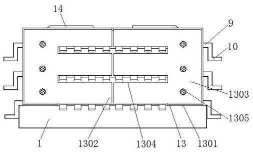
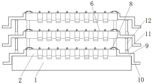
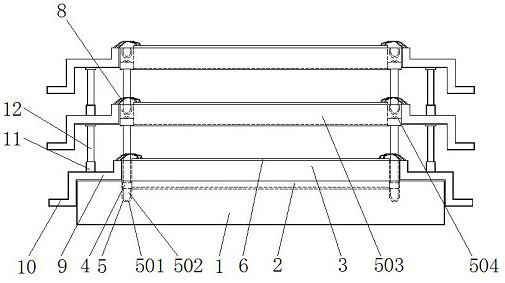
[0027] see Figure 1-5 , the present invention provides a technical solution: a multilayer hybrid semiconductor package, including a base 1, an embedding groove 2, a chip holder 3, a fixing ring 4, an erection mechanism 5, a first embedding groove 501, a double-headed embedding rod 502, Additional layer 503, hollow groove 504, second embedding groove 505, semiconductor chip 6, connecting wire plate 7, connecting wire 8, lead frame 9, pin 10, solder sleeve 11, ...


PUM


Abstract

The invention relates to a multilayer hybrid semiconductor package, which comprises a base and a sliding protection mechanism, wherein the middle part of the top end of the base is provided with an embedding groove, the middle part of the embedding groove is provided with a chip seat, the two sides of the bottom end of the chip seat are connected with fixing rings, the inner walls of the fixing rings are attached with an erection mechanism, a semiconductor chip is placed on the inner wall of the chip seat, and connecting wire boards are arranged at the top end of the semiconductor chip at equal intervals. The multilayer hybrid semiconductor package is provided with the chip seat, and the chip seat is fixedly connected with the fixing ring, so that when a user needs to install the chip seat in the embedding groove or prepares to additionally arrange the multilayer chip seat due to the packaging requirement, the user can sleeve the outer wall of the periphery of the hollowed-out groove with the fixing ring through the fixed connection formed between the fixing ring and the chip seat, so that the beneficial effect of forming multilayer erection on the chip seat is achieved, and the user can use the multilayer structure to improve diversity and diversification of different degrees for the packaging operation of a semiconductor at the moment.

Description

technical field [0001] The invention relates to the technical field of semiconductor packaging, in particular to a multilayer hybrid semiconductor packaging. Background technique [0002] Semiconductor packaging refers to the process of processing the tested wafers according to the product model and functional requirements to obtain independent chips. The packaging process is: the wafer from the wafer front-end process is cut into small chips after the dicing process, and then the cut chips are glued to the corresponding small island of the substrate frame, and then the ultra-fine Metal wires or conductive resin connect the bonding pads of the chip to the corresponding pins of the substrate to form the required circuit; then the independent chip is packaged and protected with a plastic case, and a series of operations are performed after the plastic package. After completion, the finished product is tested, usually after inspection, testing, packaging and other processes, a...

Claims


Application Information

Patent Timeline
Patent Type & Authority Applications(China)
IPC IPC(8): H01L23/04H01L23/10H01L23/31H01L23/495
CPCH01L23/04H01L23/10H01L23/49575H01L23/3107H01L2224/48247
Inventor 厉玉生陈天翼厉鹏
Owner 上海贸迎新能源科技有限公司
Why Eureka
Try Eureka