Eureka AIR delivers breakthrough ideas for toughest innovation challenges, trusted by R&D personnel around the world.

CT detector module based on deep silicon detector modules

A detector and main detector technology, applied in the field of detectors, can solve problems such as inability to provide, and achieve the effects of facilitating assembly, small size, and high counting rate

Active Publication Date: 2021-06-18
核芯光电科技(山东)有限公司
View PDF10 Cites 0 Cited by
  • Summary
  • Abstract
  • Description
  • Claims
  • Application Information

AI Technical Summary

Problems solved by technology

[0005] The above-mentioned traditional CT of the existing technology cannot provide color images and has limited spatial resolution, while the new generation of CT is limited by cadmium zinc telluride and cadmium telluride semiconductor materials with low count rate, poor stability, and high cost. The new generation of CT adopts the dislocation arrangement of the upper and lower layers and occupies a large space. The present invention provides a CT detector module based on a deep silicon detector module to solve the above technical problems

Method used


Image

  • CT detector module based on deep silicon detector modules
  • CT detector module based on deep silicon detector modules
  • CT detector module based on deep silicon detector modules

Examples


Embodiment 1

[0042] The invention provides a CT detector module based on a deep silicon detector module, including at least two deep silicon detector modules;

[0043] Each deep silicon detector module includes at least two detector chips;

[0044] Each detector chip has a light-receiving side, and the detector chips of the same deep silicon detector module are arranged in layers, and adjacent detector chips are arranged at an angle; the light-receiving sides of the same deep silicon detector module are arranged on the same arc surface, And the distance between adjacent light-receiving sides is less than the set threshold;

[0045] Each detector chip is equipped with an ASIC chip and several photoelectric units; the photoelectric unit is arranged on the light-receiving side of the detector chip, and the photoelectric units of the same detector chip form a photoelectric array, and are distributed along the edge of the light-receiving side to the inside of the detector chip ; Each photoelec...

Embodiment 2

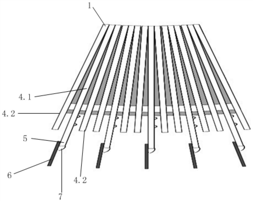
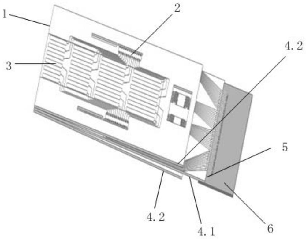
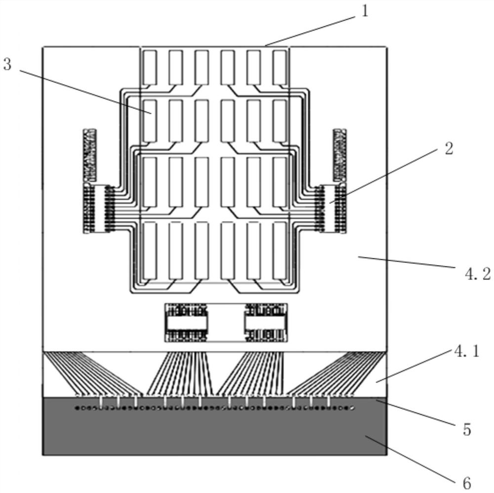
[0052] Such as figure 1 , figure 2 and image 3 As shown, the present invention provides a CT detector module based on deep silicon detector modules, including five deep silicon detector modules;

[0053] Each deep silicon detector module includes three detector chips;

[0054] Each detector chip is provided with a light-receiving side 1, and the detector chips of the same deep silicon detector module are stacked, and adjacent detector chips are arranged at an angle; the light-receiving sides 1 of the same deep silicon detector module are arranged on the same arc surface, and the distance between adjacent light-receiving sides 1 is less than the set threshold;

[0055] Each detector chip is provided with an ASIC chip 2 and a number of photoelectric units 3; Distributed to the inner side of the detector chip; each photoelectric unit 3 is connected to an input pin of the ASIC chip 2 on the same detector chip; the photoelectric unit 3 arranged on the light-receiving side 1 o...


PUM


Abstract

The invention provides a CT detector module based on deep silicon detector modules. The CT detector module comprises at least two deep silicon detector modules. Each module comprises a master detector chip and at least one slave detector chip; each of the master detector chip and the slave detector chip is provided with a light receiving side, the chips are stacked, and the adjacent chips are arranged at an angle; the light receiving sides in the same module are arranged on the same cambered surface; an integrated chip and a photoelectric unit are arranged on each of the master detector chip and the slave detector chip; the photoelectric units are arranged on the light receiving sides to form a photoelectric array, and each photoelectric unit is connected with an input pin of the corresponding integrated chip; the photoelectric units on the light receiving sides in the same module form a light receiving surface; each main chip is provided with a main output side, and the main output side is opposite to the corresponding light receiving side; each main output side is provided with a read-out PCB, and a read-out bonding pad of each read-out PCB is connected with an output pin of the corresponding integrated chip; the modules are stacked and arranged at an angle; light receiving surfaces of the modules are arranged on the same cambered surface to form a light receiving array surface; and a light shielding layer and an insulating layer are arranged between the adjacent chips.

Description

technical field [0001] The invention belongs to the technical field of detectors, and in particular relates to a CT detector module based on a deep silicon detector module. Background technique [0002] At present, the detectors used on CT are scintillator detectors. The scintillator detectors receive the X-rays that pass through the detection layer and convert them into visible light. The photodiode array receives the light signal and converts it into an electrical signal, and then converts it into a digital signal through AD conversion. , to form the final medical image after computer processing. However, the traditional CT using scintillator detectors has low imaging resolution and cannot provide color images. The equipment is bulky and heavy; and limited by the size of the detector pixels, the spatial resolution is limited. [0003] The new generation of CT uses semiconductor detection photon counters to form the detection unit of CT. The detectors use semiconductor det...

Claims


Application Information

Patent Timeline
IPC IPC(8): G01T1/161G01T1/24
CPCG01T1/161G01T1/243G01T1/246G01T1/249Y02P70/50
Inventor 刘鹏
Owner 核芯光电科技(山东)有限公司
Why Eureka
Eureka Blog
Learn More