Method for semiconductor photoetching process

A lithography process and semiconductor technology, applied in the semiconductor field, can solve the problem of heavy-duty wafers exceeding the specification line, etc., and achieve the effect of avoiding data transmission failure, avoiding operation errors, and simple operation.

Active Publication Date: 2021-06-18
CHANGXIN MEMORY TECH INC
View PDF10 Cites 1 Cited by
  • Summary
  • Abstract
  • Description
  • Claims
  • Application Information

AI Technical Summary

Problems solved by technology

[0007]The existing method of wafer rework still has the situation that the reworked wafer still exceeds the specification line

Method used


Image

  • Method for semiconductor photoetching process
  • Method for semiconductor photoetching process

Examples


Embodiment Construction

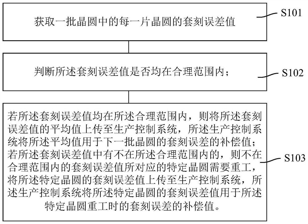
[0035] As mentioned in the background art, existing methods for reworking wafers have the situation that reworked wafers still exceed the specification line.

[0036] The study found that due to the change of the previous process or the deformation of individual wafers, the overlay error of the wafers exposed on the same chuck will be quite different. Due to the inconsistent behavior of the wafers exposed on the same chuck, the same The compensation values ​​of the wafers in the chuck are averaged, so that the wafers that need to be reworked are not optimally compensated; the reworked wafers will continue to exceed the specification line. In one embodiment, in order to solve the aforementioned problems, it is necessary to separate the measurement values ​​of the reworked wafers separately and resend them to the overlay compensation system so that the reworked wafers can be optimally compensated. This process is time-consuming. It is long, and the operation is complicated, and ...


PUM


Abstract

The invention relates to a method for a semiconductor photoetching process. The method comprises the following steps of: after acquiring an overlay error value of each wafer in a batch of wafers, judging whether the overlay error value is within a reasonable range; if all the overlay error values are within the reasonable range, uploading an average value of the overlay error values to a production control system, wherein the production control system uses the average value as a compensation value of the overlay errorsof the next batch of wafers; and if the a certain overlay error value in all of theoverlay error values is not in the reasonable range, re-machining the specific wafer corresponding to the overlay error value not in the reasonable range, and uploading the overlay error value of the specific wafer to the production control system, wherein the production control system uses the overlay error value of the specific wafer as a compensation value of the overlay error when the specific wafer is reworked. According to the method, the compensation value of the re-machined wafer can be prevented from being averaged, so that the re-machined wafer is optimally compensated, the overlay precision meets the requirement, and the method is simple to operate.

Description

technical field [0001] The invention relates to the field of semiconductors, in particular to a semiconductor photolithography process method. Background technique [0002] As a very important process in the semiconductor manufacturing process, photolithography is the process of transferring the pattern on the mask plate to the substrate through exposure, and is considered to be the core step in the manufacture of large-scale integrated circuits. A series of complex and time-consuming photolithography processes in semiconductor manufacturing are mainly completed by corresponding exposure machines. [0003] In semiconductor manufacturing, the exposure process mainly includes three major steps: the step of replacing the substrate on the chuck (stage); the step of aligning the substrate on the chuck; and the step of transferring the pattern on the mask plate to the substrate. The above three steps are repeated successively on the same chuck. [0004] In recent years, in order...

Claims


Application Information

Patent Timeline
Patent Type & Authority Applications(China)
IPC IPC(8): G03F9/00G03F7/20H01L21/66
CPCG03F9/7088G03F7/7085H01L22/24
Inventor 孙彪
Owner CHANGXIN MEMORY TECH INC
Why Eureka
Try Eureka