Cooling device, cooling method and method of manufacturing semiconductor package

A technology of cooling device and cooling method, which is applied in semiconductor/solid-state device manufacturing, semiconductor/solid-state device parts, electrical components, etc., can solve the problems of over-baking, time-consuming, difficult to form solidified film, etc., and achieve high-quality manufacturing Effect

Pending Publication Date: 2021-06-18
SCREEN HLDG CO LTD
View PDF1 Cites 0 Cited by
  • Summary
  • Abstract
  • Description
  • Claims
  • Application Information

AI Technical Summary

Problems solved by technology

As a result, it takes time to cool down the substrate on the delivery stage, so too much heat is applied to the cured film and so-called overbaking occurs
For these reasons, it is difficult to form a cured film with good film quality on the substrate, so it is difficult to form a good pattern shape and a uniform pattern size on a plane by exposing and developing the cured film.

Method used


Image

  • Cooling device, cooling method and method of manufacturing semiconductor package
  • Cooling device, cooling method and method of manufacturing semiconductor package
  • Cooling device, cooling method and method of manufacturing semiconductor package

Examples


Embodiment Construction

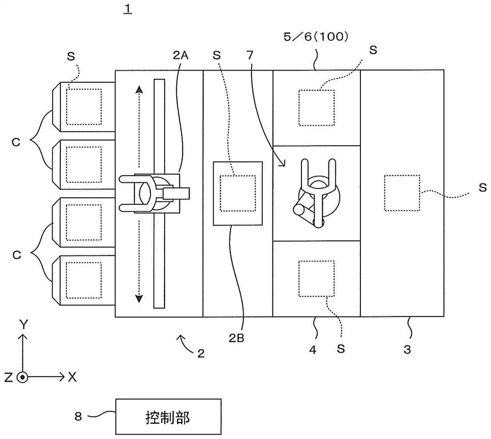
[0053] The substrate processing apparatus equipped with the cooling part which is an example of the cooling apparatus of this invention performs the pre-exposure process which is a part of manufacture of a semiconductor package, before exposing and developing a board|substrate. In particular, the substrate processing apparatus has a technical feature of cooling the substrate by a cooling unit with a correction function at the final stage of the pre-exposure process as will be described in detail later. Hereinafter, after explaining the overall structure and schematic operation of the substrate processing apparatus, the structure and operation of the cooling unit will be described in detail.

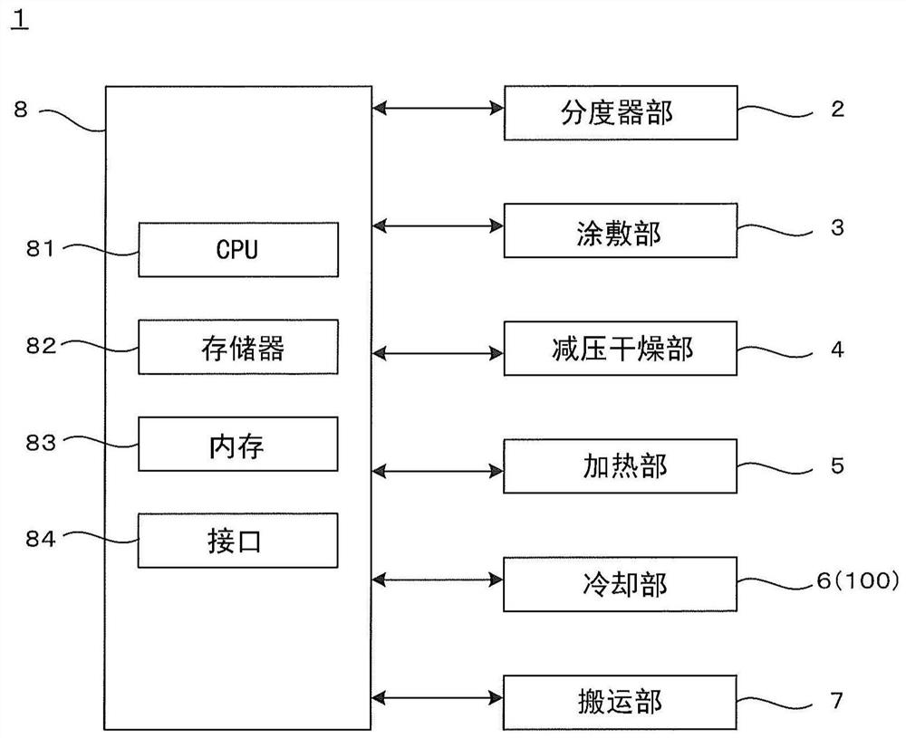
[0054] figure 1 It is a plan view showing the overall structure of a substrate processing apparatus equipped with a cooling device according to a first embodiment of the present invention. in addition, figure 2 yes means figure 1 A block diagram of the electrical structure of the subs...


PUM


Abstract

The invention provides a cooling technique capable of cooling a rectangular substrate which is subjected to heat treatment in a short time and uniformly, and a method of manufacturing a semiconductor package capable of manufacturing a high-quality semiconductor package. A cooling device comprises a cooling plate for cooling a substrate positioned at a cooling position from below; an elevating mechanism for raising and lowering a substrate between a cooling position and a standby position higher than a cooling position in a vertical direction with respect to the cooling plate; a correcting mechanism which has a correcting member which can be brought into contact with an upper surface of a peripheral part of the substrate, and corrects a peripheral part of the substrate to a cooling position by positioning a correcting member in a cooling position in the vicinity of four sides of the substrate positioned at a cooling position, thereby controlling the posture of the substrate.

Description

technical field [0001] The present invention relates to a cooling device for cooling a rectangular substrate, a cooling method, and a manufacturing method for manufacturing a semiconductor package using the substrate. Background technique [0002] In recent years, in the field of semiconductor devices, there has been a very high demand for reducing the size and thickness of devices. In order to meet such demands, panel-level fan-out packaging technology (FOPLP) that manufactures semiconductor packages using a rectangular-shaped substrate has attracted attention. In order to manufacture semiconductor packages using the FOPLP technique, it is proposed to use a substrate processing apparatus described in, for example, Japanese Patent Laid-Open No. 2019-36654. [0003] In the apparatus described in Japanese Patent Application Laid-Open No. 2019-36654, as part of semiconductor package manufacturing, the next pre-exposure process is performed before the exposure and development p...

Claims


Application Information

Patent Timeline
IPC IPC(8): H01L21/67H01L21/56
CPCH01L21/561H01L21/67005H01L21/67098H01L21/67121H01L21/67155H01L21/67207H01L23/345H01L23/367H01L23/42H01L23/473H01L23/562
Inventor 上野幸一梶屋央子
Owner SCREEN HLDG CO LTD
Why Eureka
Try Eureka