Mass production type double-sided laser direct writing photoetching machine and control method thereof

A technology of laser direct writing and lithography, which is applied in the field of exposure machines, can solve the problems of low alignment accuracy and low efficiency of integrated circuit exposure, and achieves the advantages of avoiding low alignment accuracy, improving exposure efficiency, and improving exposure alignment accuracy. Effect

Active Publication Date: 2021-06-25
HEFEI CHIP FOUND MICROELECTRONICS EQUIP CO LTD
View PDF7 Cites 0 Cited by
  • Summary
  • Abstract
  • Description
  • Claims
  • Application Information

AI Technical Summary

Problems solved by technology

[0005] For this reason, an object of the present invention is to propose a mass-produced double-sided laser direct writing lithography machine, which can expose both sides of multiple wafers in multiple regions at the same time, and solve the problem of low alignment accuracy of integrated circuit exposure. , the problem of low efficiency greatly improves the exposure production capacity, which is conducive to the mass production of integrated circuit manufacturing and wafer-level packaging

Method used


Image

  • Mass production type double-sided laser direct writing photoetching machine and control method thereof
  • Mass production type double-sided laser direct writing photoetching machine and control method thereof
  • Mass production type double-sided laser direct writing photoetching machine and control method thereof

Examples


Embodiment Construction

[0028] Embodiments of the present invention are described in detail below, and the embodiments described with reference to the drawings are exemplary, and embodiments of the present invention are described in detail below.

[0029] Refer below Figure 1-Figure 4 A mass-production double-sided laser direct writing lithography machine and a control method thereof according to an embodiment of the present invention are described.

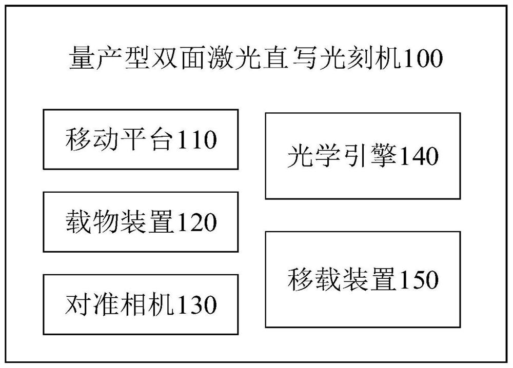
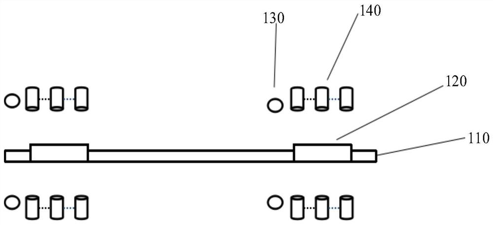
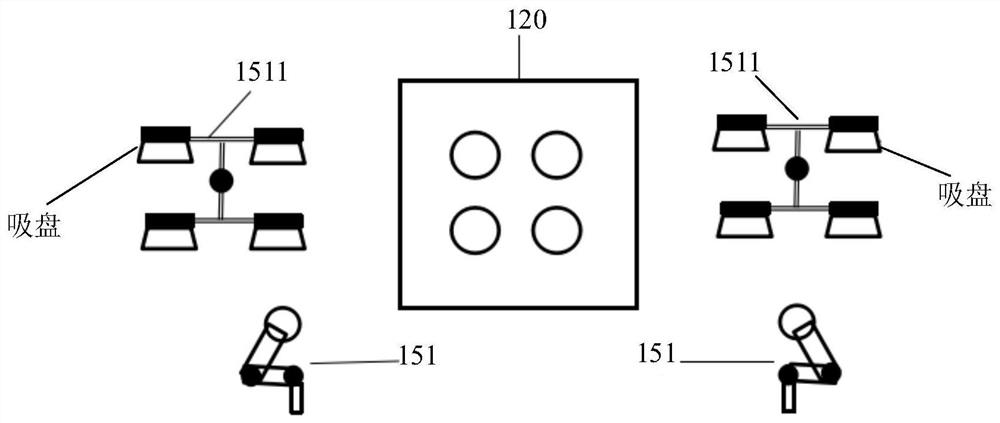
[0030] figure 1 It is a structural block diagram of a mass-production double-sided laser direct writing lithography machine according to an embodiment of the present invention. This mass-produced double-sided laser direct writing lithography machine can be applied to the manufacture of integrated circuits. It can expose both sides of multiple wafers in multiple regions at the same time, which solves the problems of low alignment accuracy and low efficiency of integrated circuit exposure. , which greatly improves the exposure production capacity, whic...


PUM


Abstract

The invention discloses a mass production type double-sided laser direct writing photoetching machine and a control method thereof. The mass production type double-sided laser direct writing photoetching machine is applied to integrated circuit manufacturing, and a mobile platform of the mass production type double-sided laser direct writing photoetching machine comprises a plurality of areas; a plurality of carrying devices are correspondingly arranged in the plurality of areas, and one or more optical engines are mounted on the upper side and the lower side of each carrying device so as to expose wafers on the carrying devices in the corresponding areas; the optical engine is provided with an alignment camera for coaxial or paraxial alignment, and an edge finder is used for performing pre-alignment processing on the position of the wafer; and the transferring device is used for transferring the wafer and transferring the wafer into or out of the carrying device in the corresponding area. Double sides of a plurality of wafers in a plurality of areas can be exposed at the same time, the problems of low exposure alignment precision and low efficiency of an integrated circuit are solved, the exposure productivity is greatly improved, and the realization of integrated circuit manufacturing and wafer level packaging mass production is facilitated.

Description

technical field [0001] The invention relates to the technical field of exposure machines, in particular to a mass-produced double-sided laser direct writing lithography machine and a control method thereof. Background technique [0002] At present, laser direct writing lithography machines are widely used in the field of integrated circuits and packaging. Due to their low production efficiency, they are mostly used in the production of mask plates and experimental lines for R&D samples in the fields of integrated circuits and packaging. Since the laser direct-write lithography machine can directly prepare computer-designed graphics on the substrate without a mask, based on the digital properties of direct-write lithography, it has higher flexibility and wide adaptability, and can be widely used to improve The efficiency of new product development meets the diverse production needs of small batches. [0003] However, the current direct-write lithography machine has low scale...

Claims


Application Information

Patent Timeline
Patent Type & Authority Applications(China)
IPC IPC(8): G03F7/20G03F9/00
CPCG03F7/70383G03F7/70716G03F7/70725G03F7/70733G03F9/7003
Inventor 曲鲁杰关远远
Owner HEFEI CHIP FOUND MICROELECTRONICS EQUIP CO LTD
Why Eureka
Try Eureka