A chip bonding method and terminal

A chip and die-bonding technology, which is applied in chip die-bonding methods and terminal fields, can solve the problems of high die-bonding cost, high consumption of testing costs, a large number of sorting costs and chip picking costs, etc., so as to save the cost of die-bonding and increase the cost of die-bonding. efficiency effect

Active Publication Date: 2022-03-25
江苏佑光科技股份有限公司
View PDF0 Cites 0 Cited by
  • Summary
  • Abstract
  • Description
  • Claims
  • Application Information

AI Technical Summary

Problems solved by technology

[0005] The problems with traditional die-bonding methods are: photoelectric testing of each chip requires a lot of testing costs; sorting the chips into different films according to the type, and selecting the corresponding film according to the type of chip required requires a lot of Sorting cost and chip picking cost, high die bonding cost and low efficiency

Method used


Image

  • A chip bonding method and terminal
  • A chip bonding method and terminal
  • A chip bonding method and terminal

Examples


Embodiment 1

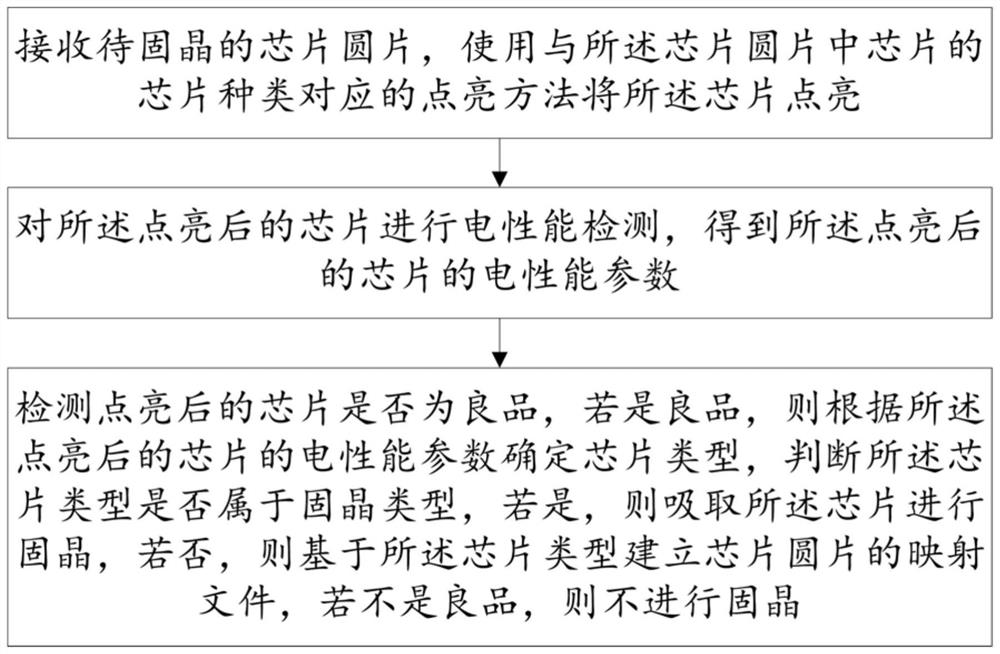
[0076] Please refer to figure 1 , a chip bonding method, comprising the steps of:

[0077] S1. Receive the chip wafer to be solidified, and use the lighting method corresponding to the chip type of the chip in the chip wafer to light up the chip;

[0078] Wherein, the types of chips include front-mounted blue-green chips, front-mounted red chips, and flip-chips;

[0079] If the type of chip is a blue-green light chip, control the electrode on the suction nozzle in the suction crystal swing arm to align with the electrode of the blue-green light chip;

[0080] If the chip type is a front-mounted red light chip, control the electrode on the suction nozzle and the electrode on the thimble in the suction crystal swing arm to align with the electrode of the front-mounted red light chip;

[0081] If the chip type is a flip chip, then control the electrode on the thimble in the suction crystal swing arm to align with the electrode of the flip chip;

[0082] Specifically, in this e...

Embodiment 2

[0099] The difference between this embodiment and Embodiment 1 is that it specifically defines how to perform secondary die-bonding on unbonded chips:

[0100] Wherein, after establishing the mapping file of the chip wafer based on the chip type, it includes:

[0101] Receive the type of chip to be bonded, automatically select the chip corresponding to the type of chip to be bonded based on the mapping file and perform the chip;

[0102] Specifically, after receiving the type of chip to be bonded, the Mapping diagram automatically selects the corresponding chip according to the type of chip to be bonded, and performs die bonding, chip arrangement, or batch transfer of chips according to the chip type, so only You need to select the chip type to bond the remaining unbonded chips, which can quickly complete the chip bonding and save the chip picking process in the bonding process, thereby improving the efficiency of bonding and reducing the cost of bonding.

Embodiment 3

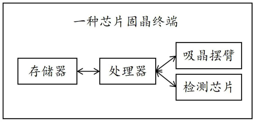
[0104] Please refer to figure 2 , a chip-bonding terminal, comprising a memory, a processor, and a computer program stored on the memory and operable on the processor, when the processor executes the computer program, the embodiment 1 or embodiment 2 is realized The various steps of the chip bonding method.

[0105] To sum up, the chip bonding method and terminal provided by the present invention receive the chip wafer to be bonded, and select the corresponding lighting method to light the chip according to the type of chip in the chip wafer. Electrodes are added to the suction nozzle and thimble of the arm, and different chip lighting methods are used for the difference in the structure of the front chip and the flip chip, so as to realize the adaptive matching of the chip lighting method according to the chip type; use the suction nozzle and the thimble to obtain the lighting The data information of the final chip is detected, and the electrical performance parameters of t...


PUM


Abstract

The invention discloses a chip bonding method and a terminal, which receive chip wafers to be bonded, select a corresponding lighting method to light the chips according to the types of chips in the chip wafers, and realize the adaptive matching of chip lighting according to the chip types. Method: conduct electrical performance detection on the lit chip, and judge whether the chip is a good product, if not, do not perform die bonding; Then the chip is sucked for die bonding. If not, the mapping file of the chip wafer is established based on the chip type. It can be seen that the mapping file of the chip wafer is established for the chip that does not belong to the bonding type, and the chips do not need to be placed separately. It can easily and intuitively read the positions of various types of chips according to the mapping file, so that the mapping file can be directly corresponded to the chip wafer during the second die bonding, which improves the die bonding efficiency and saves the cost of die bonding.

Description

technical field [0001] The invention relates to the field of crystal bonding technology, in particular to a chip bonding method and a terminal. Background technique [0002] The specific steps of the traditional die-bonding on the chip wafer are as follows: the first step is to conduct optical and electrical performance tests on the LED chips, and generate the coordinates of each chip and reference point, various optical measurement results, and various electrical measurement results. document; [0003] The second step is to import the data measured in the first step into the selection machine, set the selection rules, and align the reference points on the wafers on the selection machine. According to the classification type of electrical and optical data, select A-type, B-type, C-type chips, etc., first select one type of chip to the first empty film, and then select the next type of chip to the second empty film In this way, until the good chips on the wafer are selected...

Claims


Application Information

Patent Timeline
Patent Type & Authority Patents(China)
IPC IPC(8): H01L33/48H01L21/66H01L21/67
CPCH01L33/48H01L21/67271H01L21/67276H01L21/67288H01L22/14H01L2933/0033
Inventor 张跃春罗元明顾伟胡伟
Owner 江苏佑光科技股份有限公司
Why Eureka
Try Eureka