GaAs chip failure analysis sample and preparation method thereof

A failure analysis sample and chip technology, applied in the direction of measuring devices, instruments, measuring electronics, etc., can solve the problems that affect the failure analysis effect, the metal wiring on the chip surface is easily damaged, and the sample preparation cannot be completed.

Pending Publication Date: 2021-07-06
INTEGRA TED SERVICE TECH SHANGHAI CO LTD
View PDF0 Cites 4 Cited by
  • Summary
  • Abstract
  • Description
  • Claims
  • Application Information

AI Technical Summary

Problems solved by technology

For the GaAs chip after the HAST (accelerated aging) test, due to the influence of the HAST test conditions, the metal wiring on the chip surface has been affected. When the chemical method Decap is used to unseal the plastic package, the metal wiring on the chip surface is more It is easy to be destroyed, which will affect the subsequent failure analysis effect, or even fail to complete the sample preparation

Method used


Image

  • GaAs chip failure analysis sample and preparation method thereof
  • GaAs chip failure analysis sample and preparation method thereof
  • GaAs chip failure analysis sample and preparation method thereof

Examples


Embodiment Construction

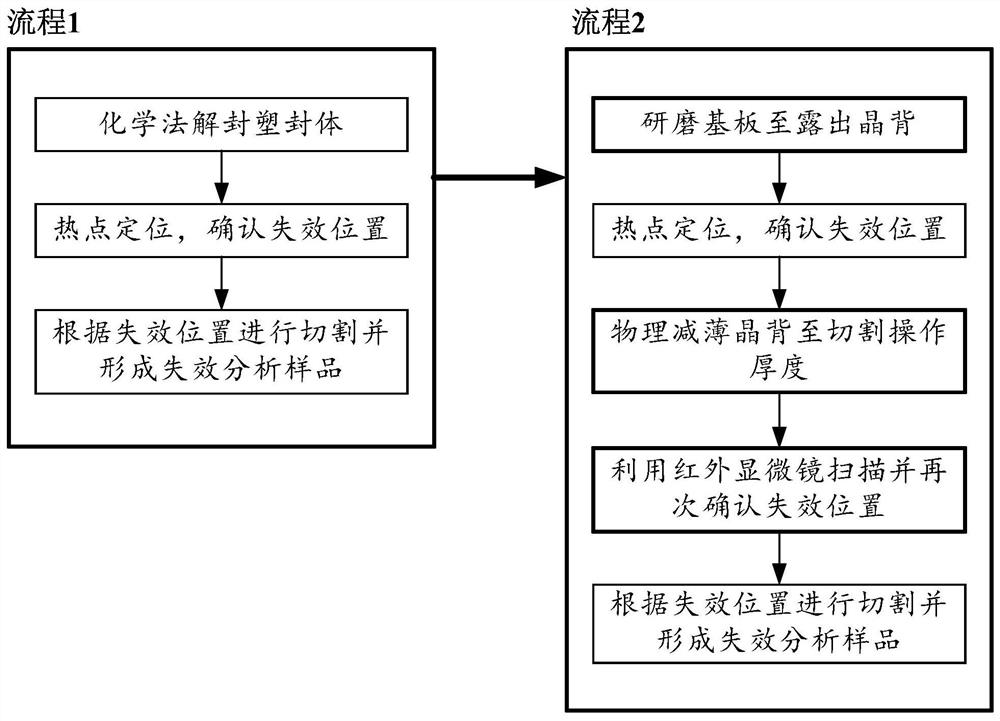
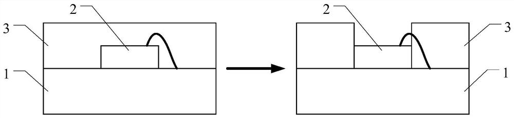
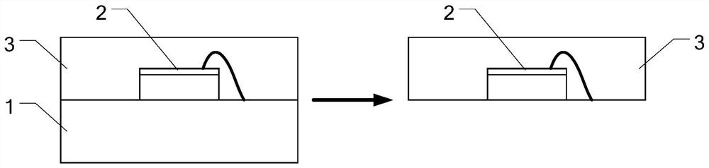
[0023] refer to figure 1 and figure 2 , figure 1 Shows the flow comparison diagram of the traditional and the GaAs chip failure analysis sample preparation method of the present invention, figure 2 It shows the state diagram of the GaAs chip before and after unpacking the plastic package by the traditional chemical method.

[0024] The GaAs chip mainly includes a substrate 1 (usually a PCB substrate) at the bottom, a chip 2 fixed on the substrate 1 , and a plastic package 3 packaged on the top and around the chip 2 . Because the wafer 2 of the GaAs chip is very thin, usually only about 200 microns in thickness, the traditional GaAs chip failure analysis sample preparation method usually uses chemical methods to unseal the plastic package, and performs hot spot location and slice inspection on the front side of the wafer 2, specifically ,like figure 1 As shown in Process 1, including steps:

[0025] Step 1, unsealing the plastic package 3 by a chemical method, exposing t...


PUM


Abstract

The invention relates to a GaAs chip failure analysis sample and a preparation method thereof. The preparation method comprises the steps of: grinding a substrate of a GaAs chip to expose the crystal back of the GaAs chip; carrying out hot spot positioning on the GaAs chip with the exposed crystal back, and confirming a failure position; physically thinning the crystal back of the GaAs chip to enable the thickness after thinning to meet the cutting operation thickness; scanning the thinned GaAs chip by using an infrared microscope, and confirming the failure position again; and cutting the thinned GaAs chip according to the failure position and forming a failure analysis sample. According to the method, a traditional chemical method for unpackaging a plastic package body is canceled, damage to metal wires of the GaAs chip is avoided, the sample preparation success rate is increased, and the subsequent failure analysis effect is guaranteed.

Description

technical field [0001] The invention relates to the technical field of semiconductors, in particular to a GaAs chip failure analysis sample and a preparation method. Background technique [0002] Because the material of GaAs (gallium arsenide) chips is easy to react with chemical reagents, the method of sample preparation for failure analysis of GaAs chips is more limited. Usually, the chemical method Decap is only used when unpacking the plastic package, but still be careful not to Destruction of the metal traces to the GaAs chip. For the GaAs chip after the HAST (accelerated aging) test, due to the influence of the HAST test conditions, the metal wiring on the chip surface has been affected. When using the chemical method Decap to unseal the plastic package, the metal wiring on the chip surface is more stable It is easy to be destroyed, which will affect the subsequent failure analysis effect, or even fail to complete the sample preparation. Contents of the invention ...

Claims


Application Information

Patent Timeline
IPC IPC(8): G01R31/26
CPCG01R31/2601
Inventor 殷荣陈佳妃
Owner INTEGRA TED SERVICE TECH SHANGHAI CO LTD
Why Eureka
Try Eureka