Check patentability & draft patents in minutes with Patsnap Eureka AI!

Optical proximity correction method, mask manufacturing method and semiconductor structure forming method

An optical proximity correction and mask technology, which is used in semiconductor/solid-state device manufacturing, optics, originals for optomechanical processing, etc., and can solve the problem that the graphics effect needs to be improved

Pending Publication Date: 2021-07-06
SEMICON MFG INT (SHANGHAI) CORP +1
View PDF0 Cites 0 Cited by
  • Summary
  • Abstract
  • Description
  • Claims
  • Application Information

AI Technical Summary

Problems solved by technology

[0004] However, the graphic effect after optical proximity correction in the prior art still needs to be improved

Method used


Image

  • Optical proximity correction method, mask manufacturing method and semiconductor structure forming method
  • Optical proximity correction method, mask manufacturing method and semiconductor structure forming method
  • Optical proximity correction method, mask manufacturing method and semiconductor structure forming method

Examples


Embodiment Construction

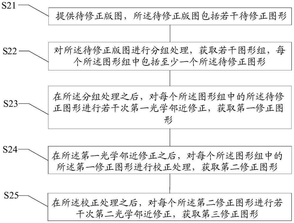
[0025] As mentioned in the background art, the graphic effect after optical proximity correction in the prior art still needs to be improved. The following will describe in detail in conjunction with the accompanying drawings.

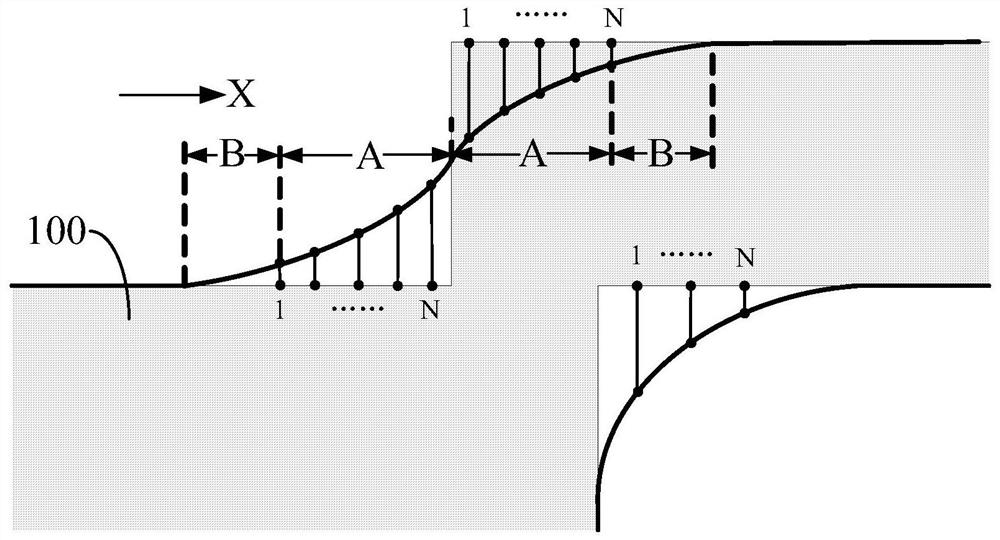
[0026] Please refer to figure 1 , provide a target layout, the target layout includes a number of target graphics 100; provide a layout to be corrected, the layout to be corrected includes a number of graphics to be corrected corresponding to the target graphics; optically perform several times on the layout to be corrected Adjacent to the correction, an intermediate layout is obtained, and the intermediate layout includes several intermediate graphics corresponding to the graphics to be corrected.

[0027] Please continue to refer figure 1 , performing exposure processing on the intermediate graphics, and obtaining the exposure graphics 101 corresponding to each of the intermediate graphics; comparing the exposure graphics 101 with the target graphi...


PUM


Abstract

The invention discloses an optical proximity correction method, a mask manufacturing method and a semiconductor structure forming method, and the method comprises the steps: providing a to-be-corrected layout which comprises a plurality of to-be-corrected patterns; grouping the to-be-corrected layout , and obtaining a plurality of graph groups, wherein each graph group comprises at least one graph to be corrected; after the grouping processing, performing first optical proximity correction on the to-be-corrected graphs in each graph group for several times, and obtaining first corrected graphs; after the first optical proximity correction, performing correction processing on the first correction graph in each graph group to obtain a second correction graph; and after the correction processing, performing a plurality of times of second optical proximity correction on each second correction graph to obtain a third correction graph. Through the technical scheme of the invention, the graphic effect of each to-be-corrected image after optical proximity correction can be improved.

Description

technical field [0001] The invention relates to the technical field of semiconductor manufacturing, in particular to an optical proximity correction method, a method for manufacturing a mask plate and a method for forming a semiconductor structure. Background technique [0002] Photolithography technology is a crucial technology in semiconductor manufacturing technology. Photolithography technology can realize the transfer of graphics from the mask to the surface of the silicon wafer to form semiconductor products that meet the design requirements. However, the existing photolithography technology is often accompanied by the optical proximity effect. [0003] In order to correct the optical proximity effect, an optical proximity correction (OPC: Optical ProximityCorrection) is produced. The core idea of ​​optical proximity correction is to establish the optical proximity correction model based on the consideration of offsetting the optical proximity effect, and design the p...

Claims


Application Information

Patent Timeline
IPC IPC(8): G03F1/36G03F7/20H01L21/027
CPCG03F1/36G03F7/70441H01L21/0274
Inventor 袁姣王伟斌王栋王兴荣
Owner SEMICON MFG INT (SHANGHAI) CORP
Features
  • R&D
  • Intellectual Property
  • Life Sciences
  • Materials
  • Tech Scout
  • Unparalleled Data Quality
  • Higher Quality Content
  • 60% Fewer Hallucinations
Learn More