Semiconductor packaging structure and preparation method thereof

A packaging structure and semiconductor technology, applied in semiconductor/solid-state device manufacturing, semiconductor devices, semiconductor/solid-state device components, etc., can solve the problems of large volume and thickness of semiconductor packaging structures, achieve precise control of height, reduce thickness and volume , Improve the effect of heat dissipation performance

Pending Publication Date: 2021-07-09
湖南越摩先进半导体有限公司
View PDF0 Cites 0 Cited by
  • Summary
  • Abstract
  • Description
  • Claims
  • Application Information

AI Technical Summary

Problems solved by technology

[0004] The defect of the traditional semiconductor package structure with antenna module is that it is necessary to form a high metal pillar in the package, and the thickness of the entire semiconductor package structure is equal to the thickness of the substrate, the height of the metal pillar and the thickness of the antenna module. resulting in larger volume and thickness of the entire semiconductor package structure

Method used


Image

  • Semiconductor packaging structure and preparation method thereof
  • Semiconductor packaging structure and preparation method thereof
  • Semiconductor packaging structure and preparation method thereof

Examples


Embodiment Construction

[0030] The present invention will be further described in detail below in conjunction with the accompanying drawings and embodiments. It should be understood that the specific embodiments described here are only used to explain the present invention, but not to limit the present invention. In addition, it should be noted that, for the convenience of description, only some structures related to the present invention are shown in the drawings but not all structures.

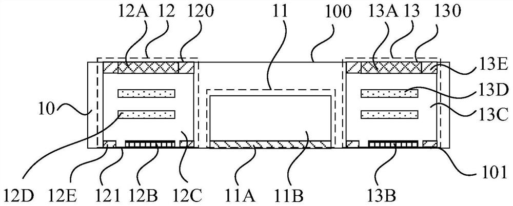
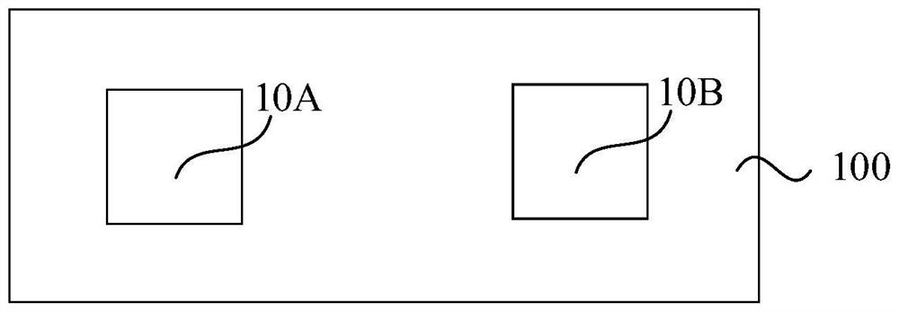
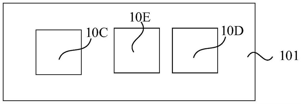
[0031] An embodiment of the present invention provides a semiconductor packaging structure. figure 1 It is a schematic structural diagram of a semiconductor package structure provided by an embodiment of the present invention. figure 2 for figure 1 Top view of the plastic enclosure. image 3 for figure 1 Bottom view of the plastic enclosure. see figure 1 , figure 2 with image 3 , the semiconductor packaging structure includes: a plastic package 10, at least one chip module 11, at least one receiving ante...


PUM


Abstract

The invention discloses a semiconductor packaging structure and a preparation method thereof. The semiconductor packaging structure comprises a plastic packaging body, at least one chip module, at least one receiving antenna module and at least one transmitting antenna module, wherein the chip module, the receiving antenna module and the transmitting antenna module are located in the plastic packaging body, and projections of the chip module, the receiving antenna module and the transmitting antenna module in the plastic packaging body are not overlapped and are spaced by a preset distance; the first surface of the receiving antenna module is provided with a receiving antenna, and the first surface of the transmitting antenna module is provided with a transmitting antenna; the second surface of the receiving antenna module is provided with a first connection bonding pad, the second surface of the transmitting antenna module is provided with a second connection bonding pad, and the surface of the chip module is provided with a third connection bonding pad. According to the technical scheme provided by the embodiment of the invention, the size and the thickness of the semiconductor packaging structure are reduced.

Description

technical field [0001] The embodiments of the present invention relate to the technical field of semiconductors, and in particular to a semiconductor packaging structure and a manufacturing method. Background technique [0002] In communication devices, chip modules and antennas need to be packaged together to form a semiconductor package structure, wherein the antenna is a device for receiving and transmitting electromagnetic wave signals, and serves as a carrier for signal transmission between different chip modules. [0003] The current conventional semiconductor package structure includes a package body provided with a chip module and an antenna module vertically stacked on the surface of the package body. Wherein, the package body includes a substrate, a chip module located on the surface of the substrate, metal pillars and plastic packaging materials. The antenna module is mounted on the surface of the package and welded on the metal post. [0004] The defect of the ...

Claims


Application Information

Patent Timeline
Patent Type & Authority Applications(China)
IPC IPC(8): H01L25/16H01L23/31H01L23/367H01L23/66H01L21/50H01L21/56H01Q1/22
CPCH01L21/50H01L21/56H01L23/3157H01L23/367H01L23/66H01L25/16H01L2223/6677H01Q1/2283
Inventor 卞龙飞
Owner 湖南越摩先进半导体有限公司
Why Eureka
Try Eureka