Supercharge Your Innovation With Domain-Expert AI Agents!

Silicon wafer cleaning equipment for solar cell processing

A technology for cleaning solar cells and silicon wafers, applied to lighting and heating equipment, cleaning methods using liquids, cleaning methods and appliances, etc., which can solve the problems of low cleaning quality and cleaning efficiency, cumbersome operation process, and prone to fragmentation and other problems, to achieve high practical value, good cleaning effect, and reduce the effect of human operation

Inactive Publication Date: 2021-07-13
TSINGHUA UNIV +1
View PDF11 Cites 0 Cited by
  • Summary
  • Abstract
  • Description
  • Claims
  • Application Information

AI Technical Summary

Problems solved by technology

[0004] The purpose of the present invention is to provide a silicon wafer cleaning equipment for solar cell processing, to solve the complex operation process of the existing silicon wafer cleaning equipment proposed in the above-mentioned background technology, the quality of cleaning and the efficiency of cleaning are relatively low, and at the same time due to The silicon wafer is relatively light and thin, and it is prone to cracking during the cleaning process, causing economic losses.

Method used


Image

  • Silicon wafer cleaning equipment for solar cell processing
  • Silicon wafer cleaning equipment for solar cell processing
  • Silicon wafer cleaning equipment for solar cell processing

Examples


Embodiment Construction

[0019] The following will clearly and completely describe the technical solutions in the embodiments of the present invention with reference to the accompanying drawings in the embodiments of the present invention. Obviously, the described embodiments are only some, not all, embodiments of the present invention. Based on the embodiments of the present invention, all other embodiments obtained by persons of ordinary skill in the art without making creative efforts belong to the protection scope of the present invention.

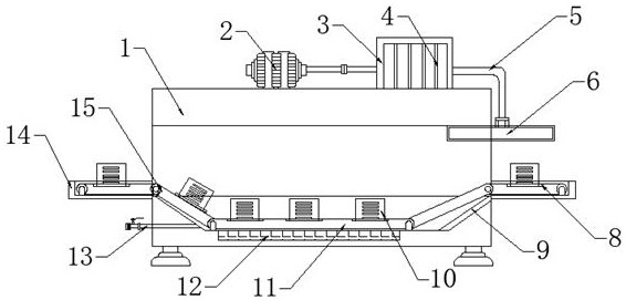
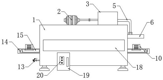
[0020] see Figure 1-5 , the present invention provides a silicon wafer cleaning device for solar cell processing, comprising a cleaning device main body 1, a cleaning tank 9 is provided at the bottom of the inner wall of the cleaning device main body 1, and the two sides of the inner wall bottom of the cleaning tank 9 are respectively conveyed with a linear belt Both sides of frame 11 bottoms are fixedly connected, and the center of bottom of inner wall of cl...


PUM


Abstract

The invention discloses silicon wafer cleaning equipment for solar cell processing. The silicon wafer cleaning equipment for solar cell processing comprises a cleaning equipment body, wherein a cleaning tank is formed in the bottom of the inner wall of the cleaning equipment body; the two sides of the bottom of the inner wall of the cleaning tank are fixedly connected with the two sides of the bottom of a linear belt conveying frame correspondingly; an ultrasonic generator is fixedly installed in the center of the bottom of the inner wall of the cleaning tank; fixing tables are fixedly arranged at the centers of the two sides of the cleaning equipment body; and belt conveyors are fixedly installed at the tops of the two fixing tables. According to the silicon wafer cleaning equipment for solar cell processing provided by the invention, an ultrasonic cleaning mode is adopted for the cleaning equipment, so that all-directional vibration cleaning can be conducted on silicon wafers, the automation degree is high, manual operation is reduced, more time and labor are saved, the cleaning effect is good, and the efficiency is high; the silicon wafers can be fixed and protected in the cleaning process, so that the occurrence of the phenomenon that the silicon wafers are broken can be greatly reduced; and the cleaned silicon wafers can be automatically dried.

Description

technical field [0001] The invention relates to the technical field of silicon wafer cleaning, in particular to a silicon wafer cleaning equipment used for solar cell processing. Background technique [0002] A solar cell is a device that directly or indirectly converts solar radiation energy into electrical energy through the photoelectric effect or photochemical effect by absorbing sunlight. The main material of most solar cell panels is "silicon wafer". Compared with ordinary batteries and rechargeable batteries, solar batteries are green products that are more energy-saving and environmentally friendly. Silicon wafers usually need to be cleaned before use, and special cleaning equipment is required at this time. [0003] The existing silicon wafer cleaning equipment has a cumbersome operation process, and the cleaning quality and cleaning efficiency are relatively low. At the same time, because the silicon wafer is relatively light and thin, it is prone to fragmentation...

Claims


Application Information

Patent Timeline
IPC IPC(8): B08B3/12F26B21/00
CPCB08B3/12F26B21/001F26B21/003
Inventor 刘一锋张志强
Owner TSINGHUA UNIV
Features
  • R&D
  • Intellectual Property
  • Life Sciences
  • Materials
  • Tech Scout
  • Unparalleled Data Quality
  • Higher Quality Content
  • 60% Fewer Hallucinations
Learn More