Semiconductor device and manufacturing method thereof

A technology of semiconductors and wide-bandgap semiconductors, which is applied in semiconductor/solid-state device manufacturing, semiconductor devices, electrical components, etc., and can solve problems such as difficulty in reducing the size of unit cells

Active Publication Date: 2021-07-13
清纯半导体(宁波)有限公司
View PDF6 Cites 0 Cited by
  • Summary
  • Abstract
  • Description
  • Claims
  • Application Information

AI Technical Summary

Problems solved by technology

However, the above structure is ...

Method used


Image

  • Semiconductor device and manufacturing method thereof
  • Semiconductor device and manufacturing method thereof
  • Semiconductor device and manufacturing method thereof

Examples


Embodiment Construction

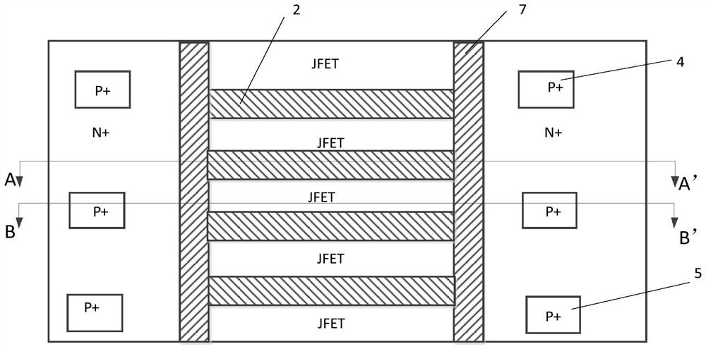
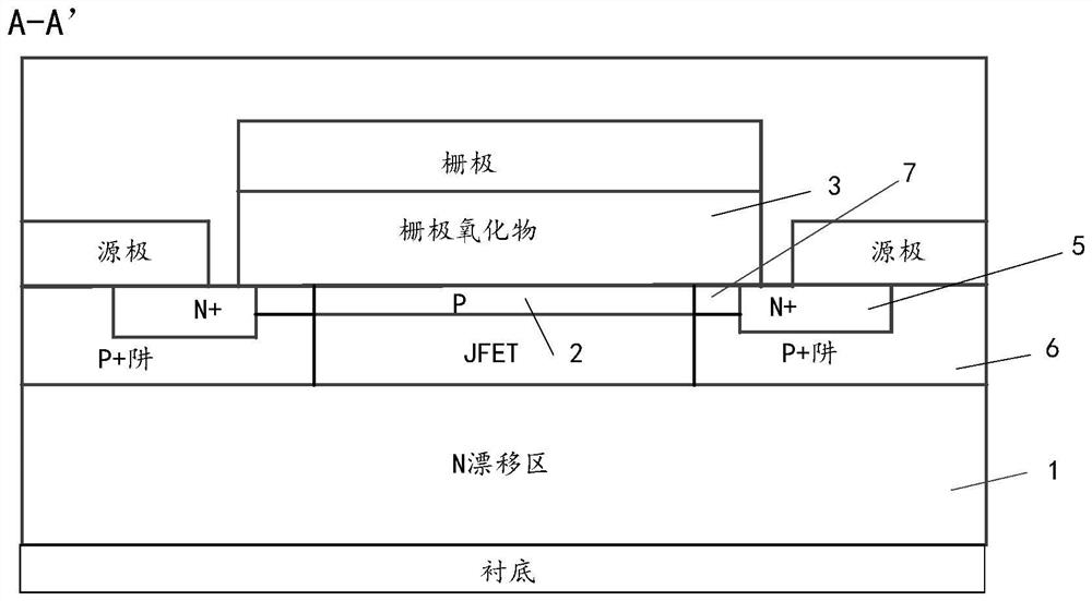
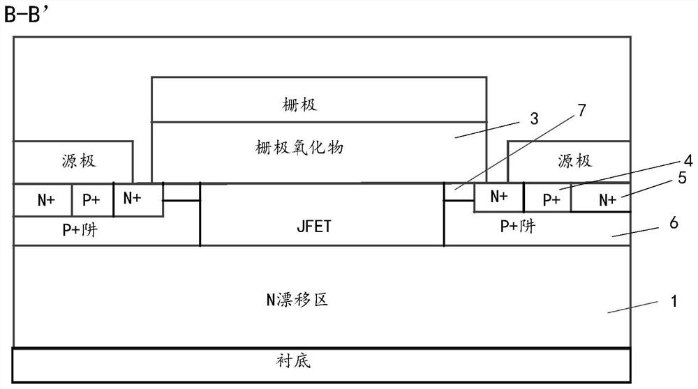
[0026] In order to make the purpose, technical solutions and advantages of the embodiments of the present invention clearer, the technical solutions in the embodiments of the present invention will be clearly and completely described below in conjunction with the drawings in the embodiments of the present invention. Obviously, the described embodiments It is a part of embodiments of the present invention, but not all embodiments. Based on the embodiments of the present invention, all other embodiments obtained by those skilled in the art without creative efforts fall within the protection scope of the present invention.

[0027] This invention may be embodied in many different forms and should not be construed as limited to the embodiments set forth herein. Rather, these embodiments are provided so that this disclosure will be thorough and complete and will fully convey the concept of the invention to those skilled in the art, and the present invention will only be defined by ...


PUM

PropertyMeasurementUnit
Doping concentrationaaaaaaaaaa
Lengthaaaaaaaaaa

Abstract

The invention discloses a semiconductor device and a manufacturing method thereof. The semiconductor device comprises: a first conductive type semiconductor layer; first semiconductor regions which are of the second conduction type and are arranged in the first conduction type semiconductor layer, wherein the first semiconductor regions extend in the first direction; and second semiconductor regions which are of a second conduction type, extend in the second direction, are arranged in the first conduction type semiconductor layer, are positioned between two adjacent first semiconductor regions and are in contact with the two adjacent first semiconductor regions. According to the semiconductor device provided by the embodiment of the invention, the widths of the junction field effect region and the second semiconductor region can be adjusted, and the unit cell size of the semiconductor device can be reduced by reducing the width of the junction field effect region.

Description

technical field [0001] The invention relates to the field of transistor structures, in particular to a semiconductor device and a manufacturing method thereof. Background technique [0002] For semiconductor devices, one potential problem is the presence of high electric fields at the gate oxide of the junction field effect (JFET) region of the device. The JFET region is typically the active part of the N-type drift region, which may include N-type dopants, and is located between the two P-type wells. The JFET region may refer to a region in contact with a channel region that reaches the surface of the P-type well by applying a gate voltage. The JFET region together with the N+ source region, the channel region, the N-type drift region, the substrate and the drain electrode constitute a conduction path for electrons. Under operating conditions where a high bias voltage is applied to the drain (close to the operating maximum) and the gate is held close to ground potential, ...

Claims


Application Information

Patent Timeline
IPC IPC(8): H01L29/06H01L29/78H01L29/739H01L21/336H01L21/331
CPCH01L29/0619H01L29/7816H01L29/7393H01L29/66681H01L29/66325
Inventor 不公告发明人
Owner 清纯半导体(宁波)有限公司
Why Eureka
Try Eureka