P-band three-dimensional broadband composite wave-absorbing metamaterial and preparation method thereof
A broadband and P-band technology is applied in the field of P-band three-dimensional broadband composite absorbing metamaterial and its preparation, which can solve the problems of undocumented absorbing effect and high energy consumption of absorbing materials, and is beneficial to engineering applications, The effect of good absorption effect and easy wave absorption performance
- Summary
- Abstract
- Description
- Claims
- Application Information
AI Technical Summary
Problems solved by technology
Method used
Image
Examples
Embodiment 1
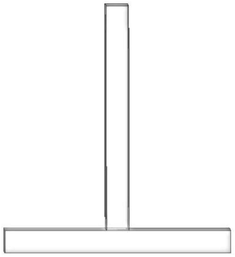
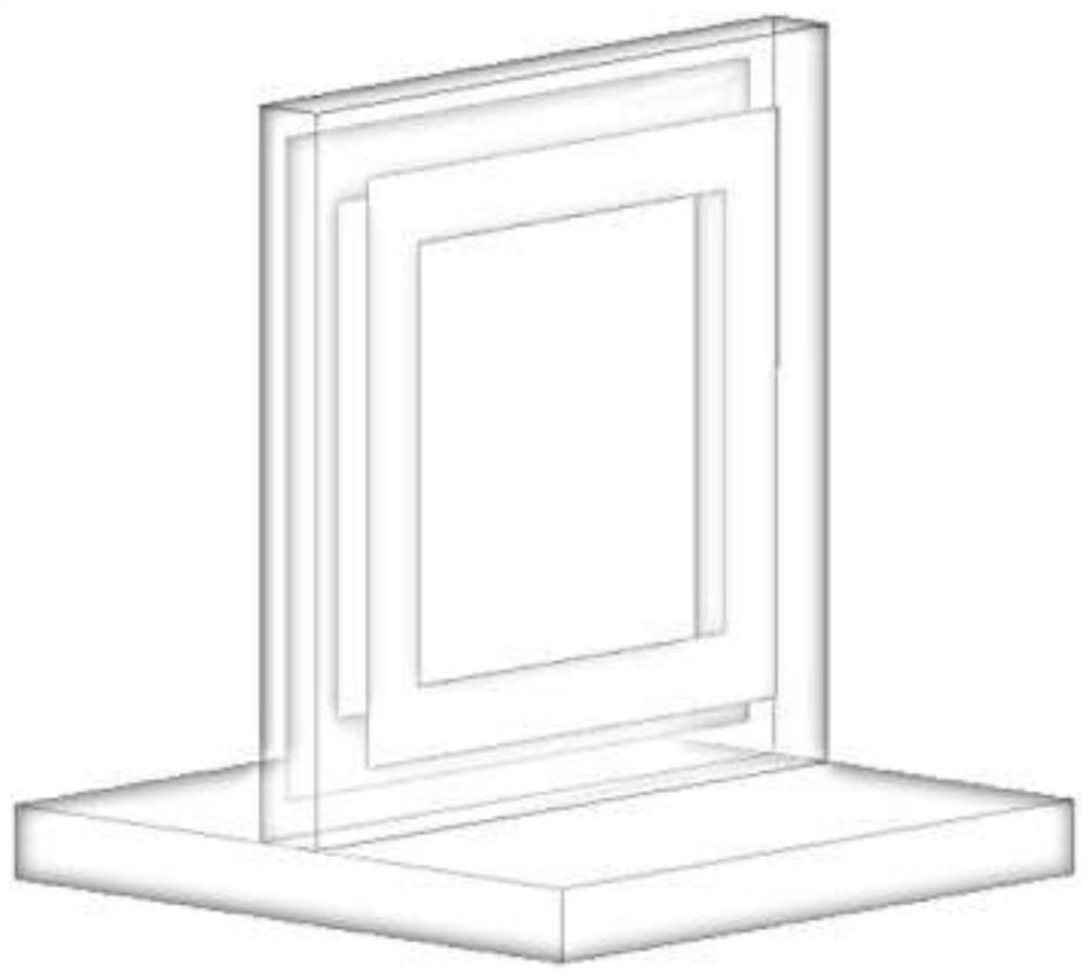
[0046] In this embodiment, the P-band three-dimensional broadband composite wave-absorbing metamaterial is composed of metal-type electromagnetic metamaterial structural units based on magnetic metal iron, which are periodically vertically arranged on the manganese-zinc ferrite dielectric substrate; the metal-type electromagnetic metamaterial The structural unit consists of two square metal rings of different sizes placed on the front and back sides of an FR4 dielectric substrate with a thickness of 2mm and a dielectric constant of 4.2; the thickness of the square metal rings is 35 microns, and the outer length of the front square ring is 55mm, the inner side length is 50mm; the outer side length of the reverse square ring is 52mm, and the inner side length is 45mm.
[0047] The preparation method of the P-band three-dimensional broadband composite wave-absorbing metamaterial in this embodiment includes the following steps:
[0048] (1) Ferrite material cutting
[0049] Cut the...
Embodiment 2
[0061] In this embodiment, the P-band three-dimensional broadband composite wave-absorbing metamaterial is periodically vertically arranged on the nickel-zinc ferrite dielectric substrate by the structural units of the metal-type electromagnetic metamaterial based on magnetic metal nickel; the metal-type electromagnetic metamaterial The structural unit is composed of two square metal rings of different sizes placed on the front and back sides of the FR4 dielectric substrate with a thickness of 2.5mm and a dielectric constant of 4.2; the thickness of the square metal ring is 30 microns, and the outer side of the front square ring The length is 55mm, and the length of the inner side is 50mm; the length of the outer side of the reverse square ring is 52mm, and the length of the inner side is 45mm.
[0062] The preparation method of the P-band three-dimensional broadband composite wave-absorbing metamaterial in this embodiment includes the following steps:
[0063] (1) Ferrite mat...
Embodiment 3
[0076] In this embodiment, the P-band three-dimensional broadband composite wave-absorbing metamaterial is periodically erected on the magnesium-zinc ferrite dielectric substrate by the structural unit of the metal-type electromagnetic metamaterial based on magnetic metal cobalt; the structural unit of the metal-type electromagnetic metamaterial Two square metal rings of different sizes are placed on the front and back sides of an FR4 dielectric substrate with a thickness of 2.5mm and a dielectric constant of 3.5; the thickness of the square metal ring is 25 microns, and the outer length of the front square ring is 55mm, the inner side length is 45mm; the outer side length of the reverse square ring is 50mm, and the inner side length is 42mm.
[0077] The preparation method of the P-band three-dimensional broadband composite wave-absorbing metamaterial in this embodiment includes the following steps:
[0078] (1) Ferrite material cutting
[0079] Cut the ferrite dielectric ma...
PUM
| Property | Measurement | Unit |
|---|---|---|
| thickness | aaaaa | aaaaa |
| thickness | aaaaa | aaaaa |
| thickness | aaaaa | aaaaa |
Abstract
Description
Claims
Application Information


