High-voltage silicon stack alloy processing device and alloying method

A processing device, high-pressure silicon stacking technology, applied in metal processing equipment, manufacturing tools, non-electric welding equipment, etc., can solve the problems of scrapped alloy workpieces, unstable pressure, large loss of raw materials, etc., to achieve uniform thickness and regularity, down pressure The action is smooth and gentle, and the effect of improving the strength of the solder tab

Pending Publication Date: 2021-07-23
YANGZHOU YANGJIE ELECTRONIC TECH CO LTD
View PDF0 Cites 0 Cited by
  • Summary
  • Abstract
  • Description
  • Claims
  • Application Information

AI Technical Summary

Problems solved by technology

However, in this alloy method, the compressed air connected to the cylinder is continuously opened, and the pressure output from the air supply pipeline connected to the cylinder to the cylinder of the alloy machine is not stable, and may fluctuate due to interference from other connected equipment
This kind of gas supply fluctuation will cause the pressure of the cylinder, piston and cylinder to fluctuate. Before the solder is heated to the liquidus temperature, the impact of the pressure change is not obvious; but after the solder is heated to the liquidus temperature, the sudden increase of the air pressure The increase will make the workpiece overpressure, the solder overflows, and the bonding area is too thin, resulting in the overall scrap of the alloy workpiece and a huge loss of raw materials

Method used


Image

  • High-voltage silicon stack alloy processing device and alloying method
  • High-voltage silicon stack alloy processing device and alloying method

Examples


Embodiment Construction

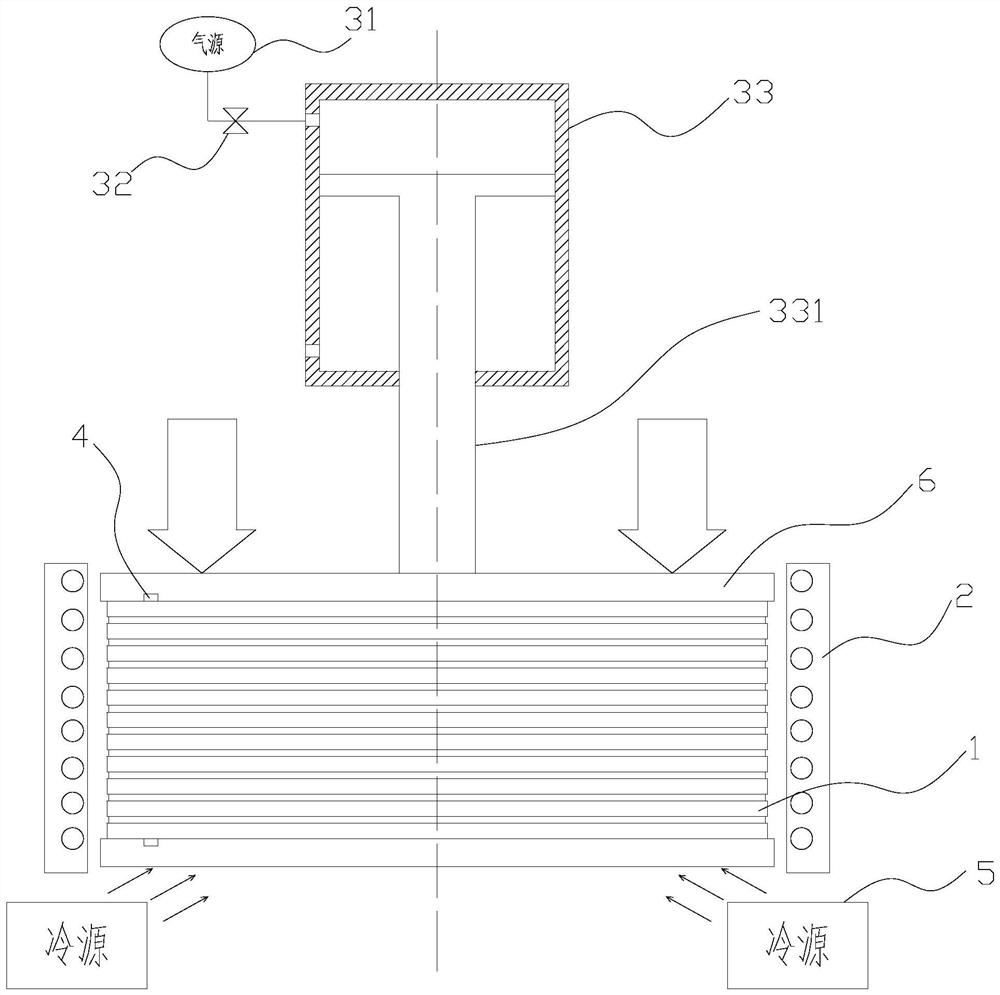
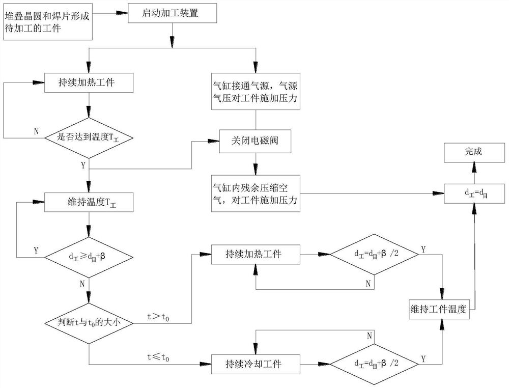
[0031] The following is attached Figure 1-2 , to further illustrate the present invention.

[0032] A high-pressure silicon stack alloy processing device of the present invention includes a workpiece 1, an annular electromagnetic heating device 2 and a workpiece thickness monitoring unit, and also includes a pressure unit, a temperature sensor 4 and a controller;

[0033] The workpiece 1 is formed by stacking several wafers and several welding pieces in an interlaced manner; the workpiece 1 is placed inside the annular electromagnetic heating device 2;

[0034] The pressure unit includes an air source 31 and a cylinder 33, and the air source 31 and the cylinder 33 are connected through an air supply pipeline, and an electromagnetic valve 32 is also arranged on the air supply pipeline, and the electromagnetic valve 32 is used to control the opening and closing of the air supply channel;

[0035] The upper and lower surfaces of the workpiece 1 are provided with a lining plate ...


PUM


Abstract

The invention discloses a high-voltage silicon stack alloy processing device and an alloying method. The invention relates to the technical field of semiconductor processing, in particular to the high-voltage silicon stack alloy processing device and the alloying method. The high-voltage silicon stack alloy processing device comprises a workpiece, an annular electromagnetic heating device, a workpiece thickness monitoring unit, a pressure unit, a temperature sensor and a controller; the workpiece is formed by alternatively stacking a plurality of wafers and a plurality of soldering lugs; the workpiece is placed in the annular electromagnetic heating device; the pressure unit comprises an air source and an air cylinder, the air source is communicated with the air cylinder through an air supply pipeline, and an electromagnetic valve is further arranged on the air supply pipeline; and the annular electromagnetic heating device, the workpiece thickness monitoring unit, the temperature sensor, the air cylinder and the electromagnetic valve are all in communication connection with the controller. By means of the high-voltage silicon stack alloy processing device, the strength of the soldering lugs is improved, the downward pressing process is delayed, and it is ensured that the soldering lugs in an alloy have the uniform thickness and the regular form.

Description

technical field [0001] The invention relates to the technical field of semiconductor processing, in particular to a high-voltage silicon stack alloy processing device and alloy method. Background technique [0002] The processing of high-voltage silicon stack diodes is made by cross-stacking several layers of wafers and several layers of solder (solder sheets), heating and pressing to form an integrated alloy block, and then cutting the alloy block into several unit silicon columns. . [0003] In alloy production, the high-frequency alloy machine commonly used at present uses compressed air as the power cylinder to provide pressure for the workpiece. During the pressurization process, it is heated to the solder liquidus temperature, so that several wafers are connected by solder bonding to achieve the purpose of alloy operation. However, in this alloy method, the compressed air connected to the cylinder is continuously opened, and the pressure output from the air supply pi...

Claims


Application Information

Patent Timeline
Patent Type & Authority Applications(China)
IPC IPC(8): B23K20/02
CPCB23K20/023
Inventor 王永彬王毅
Owner YANGZHOU YANGJIE ELECTRONIC TECH CO LTD
Why Eureka
Try Eureka