
Variable-focal-length semiconductor surface micro lens, manufacturing method thereof and laser

A manufacturing method and microlens technology, which can be applied to semiconductor lasers, lasers, laser parts, etc., can solve the problems of optical uniformity of surface microlenses, high cost, and poor product yield.

Active Publication Date: 2021-07-30
VERTILITE CO LTD
View PDF5 Cites 1 Cited by
  • Summary
  • Abstract
  • Description
  • Claims
  • Application Information

AI Technical Summary

Problems solved by technology

[0002] In the field of semiconductor surface microlens technology, in order to produce a long focal length microlens structure, it is usually necessary to rely on a surface microlens process with a large curvature, that is, it is necessary to use high-precision Surface microlens etching process, high cost
Moreover, even if a high-precision surface microlens etching process is used to manufacture a microlens structure with a long focal length, if microlenses with different etching depths are made on the surface of the semiconductor at the same time to make microlenses with different long focal lengths, it will also affect the semiconductor. The optical uniformity of the surface microlens is affected, resulting in poor overall product yield

Method used


Image

  • Variable-focal-length semiconductor surface micro lens, manufacturing method thereof and laser
  • Variable-focal-length semiconductor surface micro lens, manufacturing method thereof and laser
  • Variable-focal-length semiconductor surface micro lens, manufacturing method thereof and laser

Examples


Embodiment Construction

[0028] The present invention will be further described in detail below in conjunction with the accompanying drawings and embodiments. It should be understood that the specific embodiments described here are only used to explain the present invention, but not to limit the present invention. In addition, it should be noted that, for the convenience of description, only some structures related to the present invention are shown in the drawings but not all structures.

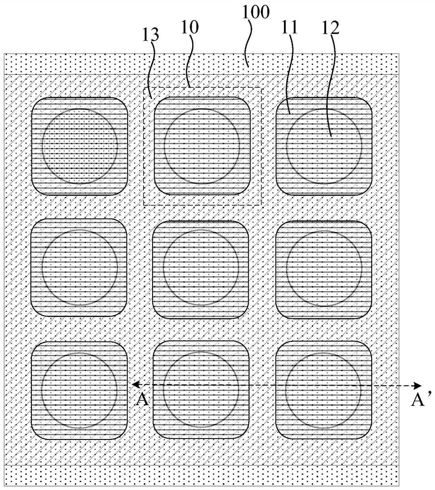
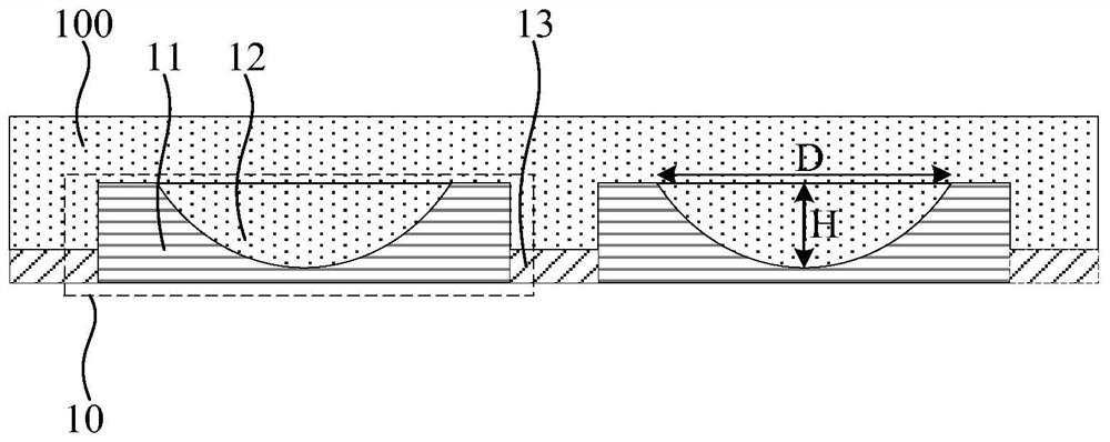
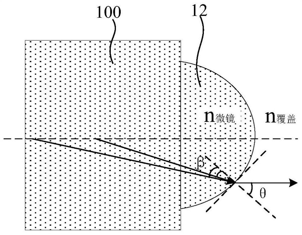
[0029] figure 1 It is a schematic structural diagram of a variable focal length semiconductor surface microlens provided by an embodiment of the present invention, figure 2 Yes figure 1 Sectional view along line AA', combined with figure 1 and figure 2 , the variable focal length semiconductor surface microlens comprises: substrate 100; Lens unit 10, is positioned at the side of substrate 100; Lens unit 10 comprises microlens 12 and zoom layer 11, and zoom layer 11 is positioned at microlens 12 away from subs...


PUM


Abstract

The embodiment of the invention discloses a variable-focal-length semiconductor surface micro lens, a manufacturing method thereof and a laser. The variable focal length semiconductor surface microlens includes a substrate and a lens unit, wherein the lens unit is located on one side of the substrate; the lens unit comprises a micro lens and a varifocal layer, the varifocal layer is located on the side, away from the substrate, of the micro lens and covers the light-emitting surface of the micro lens, and the varifocal layer is used for adjusting the refractive index of the lens unit; the refractive index of the lens unit is difference between the refractive index of the micro lens and the refractive index of the varifocal layer. According to the micro lens, the variable focal length of the surface micro lens is realized, namely, different focal lengths of the micro lens are realized, the method is simple and practical, dependence on a high-precision surface micro lens etching process when a long-focal-length micro lens is realized is avoided, cost is low, and meanwhile, the overall product yield is ensured.

Description

technical field [0001] Embodiments of the present invention relate to semiconductor surface microlens technology, in particular to a semiconductor surface microlens with variable focal length, a manufacturing method thereof, and a laser. Background technique [0002] In the field of semiconductor surface microlens technology, in order to produce a long focal length microlens structure, it usually needs to rely on a surface microlens process with a large curvature, that is, a high-precision surface microlens etching process is required, and the cost is high. Moreover, even if a microlens structure with a long focal length is made by using a high-precision surface microlens etching process, if microlenses with different etching depths are made on the surface of the semiconductor at the same time to make microlenses with different long focal lengths, it will also affect the semiconductor. The optical uniformity of the surface microlens is affected, resulting in poor overall pro...

Claims


Application Information

Patent Timeline
IPC IPC(8): G02B3/00H01S5/02253
CPCG02B3/00G02B3/0012G02B3/0037
Inventor 彭俊彦翁玮呈刘嵩梁栋
Owner VERTILITE CO LTD
Learn More