High-speed Tracking Method for Micro-Nano Structure Pattern Sample

A technology of micro-nano structure and graphics, which is applied in the direction of image communication, color TV parts, TV system parts, etc., can solve problems such as instability, and achieve high tracking accuracy and high tracking sensitivity.

Active Publication Date: 2022-05-31
SHANGHAI INST OF OPTICS & FINE MECHANICS CHINESE ACAD OF SCI
View PDF10 Cites 0 Cited by
  • Summary
  • Abstract
  • Description
  • Claims
  • Application Information

AI Technical Summary

Problems solved by technology

[0003] The purpose of the present invention is to overcome the unstable problem of the existing astigmatism automatic tracking technology when tracking the micro-nano structure graphics, and judge whether the current position is in the graphics area or the non-graphics area before real-time tracking

Method used


Image

  • High-speed Tracking Method for Micro-Nano Structure Pattern Sample
  • High-speed Tracking Method for Micro-Nano Structure Pattern Sample
  • High-speed Tracking Method for Micro-Nano Structure Pattern Sample

Examples


Embodiment 1

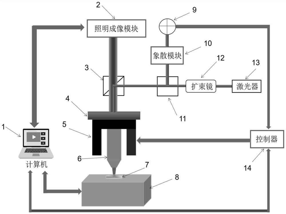
[0032] like figure 1 As shown in the figure, the high-speed tracking method for imaging the micro-nano structure pattern sample includes a computer 1, an illumination imaging module 2, a dichroic prism 3, a focusing mechanism 4, a piezoelectric ceramic 5, an objective lens 6, and a micro-nano structure pattern test sample to be tracked. Sample 7 , workpiece stage 8 , detector 9 , astigmatism module 10 , beam splitting module 11 , beam expander 12 , laser 13 and controller 14 . Place the micro-nano structure pattern sample 7 to be tracked on the workpiece stage 8, and move the focusing mechanism 4 up and down, so that the surface of the micro-nano structure pattern sample 7 to be tracked is clearly imaged on the illumination imaging module 2 and set as the focus . Adjust the beam expander 12 so that the laser light emitted by the laser 13 is focused on the surface of the sample 7 with the micro-nano structure pattern to be tracked, and control the workpiece stage 8 and the con...


PUM


Abstract

A high-speed tracking method for micro-nano-structure graphic samples, including a computer, an illumination imaging module, a dichroic prism, a focusing mechanism, piezoelectric ceramics, an objective lens, a micro-nano-structure graphic sample to be tracked, a workpiece table, a detector, an image Diffusion module, beam splitter module, beam expander, laser and controller. The micro-nano structure pattern sample to be tracked is placed on the workpiece table, and the surface of the micro-nano structure pattern sample to be tracked is clearly imaged in the illumination imaging module by moving the focusing mechanism up and down. Adjust the beam expander so that the laser emitted by the laser is focused on the surface of the micro-nano structure pattern sample to be tracked, and the workpiece table and the controller are synchronously controlled to complete the movement and tracking of the micro-nano structure pattern sample to be tracked. The high-speed tracking method of the micro-nano structure pattern sample of the present invention can automatically track the micro-nano structure pattern sample at high speed, high precision and high sensitivity, so as to ensure clear imaging of the micro-nano structure pattern and provide guarantee for subsequent reading and detection.

Description

technical field [0001] The invention relates to the field of high-speed tracking of micro-nano structure pattern samples, and is a novel tracking control method based on astigmatic defocus detection, which can be used for high-speed tracking of micro-nano structure pattern samples during imaging. Background technique [0002] Whether the optical device with micro-nano structure can meet the design parameters is mainly affected by the micro-nano structure, so the detection of micro-nano structure pattern sample imaging is very important. When historical documents such as ancient books and paintings, classical masterpieces, and archives are preserved at the micro-nano level, whether they can quickly read such micro-nano-level images and text information determines the efficiency of this preservation method. However, when detecting or reading micro-nano-level structures, it is necessary to use high-magnification objective lenses, which have small field of view and depth of fiel...

Claims


Application Information

Patent Timeline
Patent Type & Authority Patents(China)
IPC IPC(8): H04N5/232H04N5/225H04N5/235G01N21/01
CPCG01N21/01H04N23/50H04N23/55H04N23/67H04N23/70
Inventor 刘星魏劲松陈国东郑金轮赵培均
Owner SHANGHAI INST OF OPTICS & FINE MECHANICS CHINESE ACAD OF SCI
Why Eureka
Try Eureka