Ultraviolet wide-spectrum maskless photoetching imaging system and photoetching machine

A maskless lithography and imaging system technology, applied in the field of ultraviolet wide-spectrum maskless lithography imaging systems and lithography machines, can solve the problems of difficult correction of chromatic aberration of magnification, low transmittance, small depth of focus, etc., to achieve High operational stability, high transmittance, and strong adaptability

Active Publication Date: 2021-08-06
HEFEI CHIP FOUND MICROELECTRONICS EQUIP CO LTD
View PDF0 Cites 1 Cited by
  • Summary
  • Abstract
  • Description
  • Claims
  • Application Information

AI Technical Summary

Problems solved by technology

[0003] In related technologies, there are problems such as high cost, low transmittance, difficult correction of chromatic aberration of magnification, and small depth of focus in the ultraviolet wide-spectrum maskless lithography imaging system in t

Method used


Image

  • Ultraviolet wide-spectrum maskless photoetching imaging system and photoetching machine
  • Ultraviolet wide-spectrum maskless photoetching imaging system and photoetching machine
  • Ultraviolet wide-spectrum maskless photoetching imaging system and photoetching machine

Examples


Example Embodiment

[0051] Embodiments of the present invention will be described in detail below, and embodiments of the present invention will be described in detail below with reference to the embodiments described in detail below.

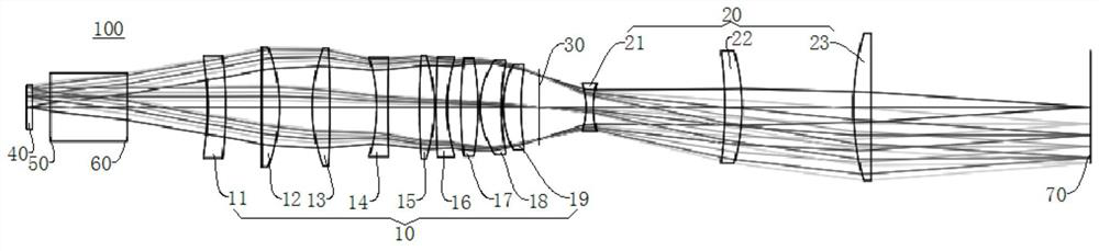
[0052] Below Figure 1 - Figure 4 A ultraviolet wide spectroscopy, an ultraviolet wide spectroscopy, in accordance with an embodiment of the present invention, an ultraviolet wide spectrum-free mask photolithography imaging system 100 includes a first lens assembly 10, a stop 30, and a second lens assembly 20. The following is applied to the photolithography machine as an example of an ultraviolet width spectroscopy as an example, but does not use a limit to this.

[0053] Specifically, if figure 1 As shown, the first lens assembly 10 includes: a first lens 11, a second lens 12, a third lens 13, a fourth lens 14, a fifth lens 15, a sixth lens 16, a seventh lens 17, an eighth lens 18, The ninth lens 19, the second lens assembly 20 includes: tenth lens 21, the eleventh l...


PUM


Abstract

The invention discloses an ultraviolet wide-spectrum maskless photoetching imaging system and a photoetching machine. The ultraviolet wide-spectrum maskless photoetching imaging system comprises a first lens assembly, a diaphragm and a second lens assembly, the focal length of the first lens assembly is f1, the focal length of the second lens assembly is f2, the focal length of the ultraviolet wide-spectrum maskless photoetching imaging system is f, and the ultraviolet wide-spectrum maskless photoetching imaging system meets the following relational expressions: 0.05 <= f1/f <= 0.09, and 0.21 <= f2/f <= 0.41; and the first lens to a twelfth lens are sequentially arranged from the object side to the image side along the optical axis, and the first lens to the twelfth lens are all single lenses. According to the ultraviolet wide-spectrum maskless photoetching imaging system, a light source with a wider wave band can be adopted, the design of high imaging quality, large focal depth and high transmittance is realized by using a small number of lenses, a balsaming lens is not adopted, so that the optical imaging system is more stable, the photoetching cost is reduced, and the photoetching equipment has higher operation stability.

Description

technical field [0001] The invention relates to the technical field of optical imaging, in particular to an ultraviolet wide-spectrum maskless photolithography imaging system and a photolithography machine. Background technique [0002] PCB (Printed Circuit Board, printed circuit board) is an important carrier for the electrical connection of electronic components. At present, consumer electronic products such as mobile phones and computers are developing in the direction of light, small and multi-functional, which also makes PCB gradually develop in the direction of higher density layout, and lithography equipment such as maskless lithography machine is a high-precision PCB The required core equipment, which uses DMD (Digital Micromirror Device, digital micromirror device) to replace the mask plate required by traditional lithography equipment, so that the exposure accuracy is no longer affected by the mask plate, while reducing the cost of using the mask plate . The expo...

Claims


Application Information

Patent Timeline
IPC IPC(8): G03F7/20G02B13/00G02B13/22
CPCG03F7/7015G02B13/005G02B13/22
Inventor 李鹏飞杨宇航蔡潍戚蓉蓉
Owner HEFEI CHIP FOUND MICROELECTRONICS EQUIP CO LTD
Why Eureka
Try Eureka