Display panel and display device
A technology for display panels and substrates, which is applied to semiconductor devices, electrical components, circuits, etc., can solve problems such as the reduction of luminous efficiency, and achieve the effects of improving luminous efficiency, reducing luminous flux, and improving contrast.
- Summary
- Abstract
- Description
- Claims
- Application Information
AI Technical Summary
Problems solved by technology
Method used
Image

Examples
Embodiment 1
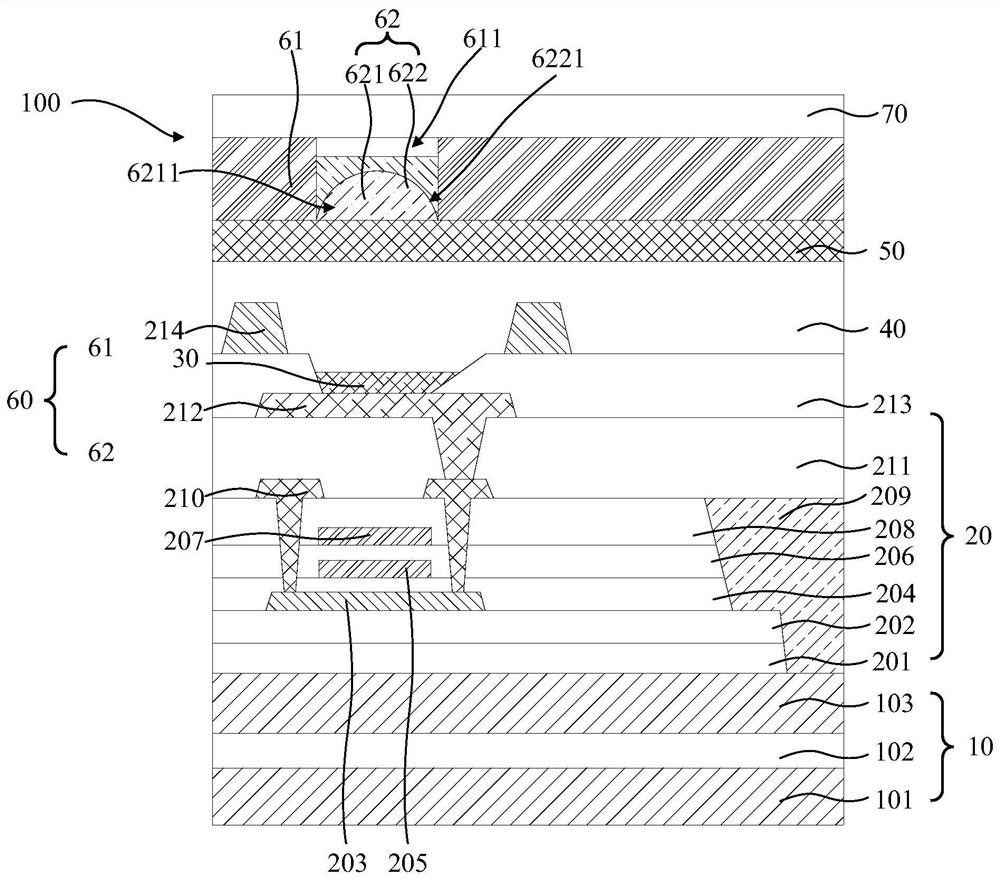
[0034] Such as figure 1 As shown in , it is a cross-sectional structure diagram of the display panel provided by the first embodiment of the present application.
[0035] The display panel 100 provided in the embodiment of the present application may include a substrate 10 , an array structure layer 20 located on the substrate 10 , a light emitting functional layer 30 located on the array structure layer 20 , a light emitting functional layer located on the light emitting functional layer 30 The thin film encapsulation layer 40 , the touch layer 50 and the cover layer 70 located on the thin film encapsulation layer 40 .
[0036] In this embodiment, the light-emitting functional layer 30 includes a plurality of light-emitting devices, one of the light-emitting devices corresponds to one of the first openings 611, and the outgoing light emitted by the light-emitting devices is guided out to the The display panel 100 is described.
[0037] Specifically, an optical adjustment la...
Embodiment 2
[0051] Specifically, this embodiment is the same or similar to Embodiment 1, the only difference is:
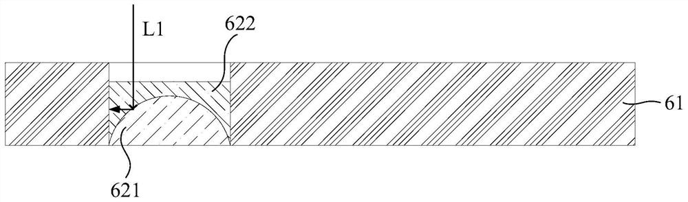
[0052] Such as image 3 As shown in , it is a cross-sectional structure diagram of the display panel provided by the second embodiment of the present application.
[0053] In this embodiment, the dimming unit 62 includes a first transparent layer 621 and a second transparent layer 622 located on the first transparent layer 621, and the second transparent layer 622 is far away from the first transparent layer. A surface on one side of the transparent layer 621 is located on the same plane as a surface of the black matrix 61 on a side away from the substrate 10 . The advantage of this arrangement is to effectively avoid external water vapor remaining on the interface between the dimming unit 62 and the black matrix 61, thereby reducing the erosion of the external water vapor on the interface between the dimming unit 62 and the black matrix 61 .
[0054] In view of the techni...
Embodiment 3
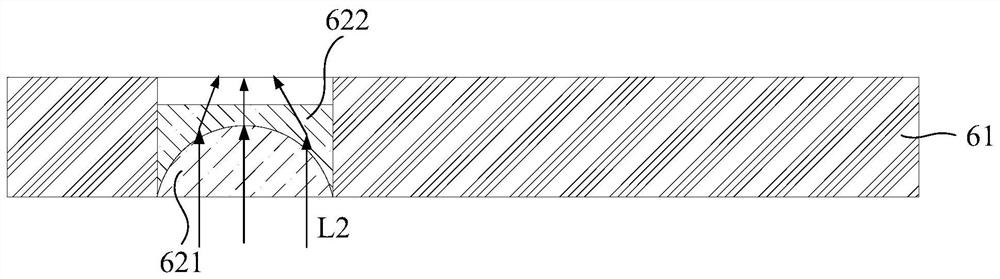
[0056] Such as Figure 4 As shown in FIG. 1 , is a cross-sectional structure diagram of the display panel provided by the third embodiment of the present application.
[0057] In the embodiment of the present application, the dimming unit 62 includes a first transparent layer 621 and a second transparent layer 622 located on the first transparent layer 621, the second transparent layer 622 is far away from the The substrate 10 is provided; wherein, the refractive index of the first transparent layer 621 is smaller than the refractive index of the second transparent layer 622 .
[0058] In the embodiment of the present application, at least one first protrusion 6211 is provided on the surface of the first transparent layer 621 away from the substrate 10, and the second transparent layer 622 is close to the first transparent layer. One side of the optical layer 621 has a first groove 6221 corresponding to the first protrusion 6211 . The first protrusions 6211 can reflect the r...
PUM
| Property | Measurement | Unit |
|---|---|---|
| thickness | aaaaa | aaaaa |
Abstract
Description
Claims
Application Information
 - R&D
- Intellectual Property
- Life Sciences
- Materials
- Tech Scout
- Unparalleled Data Quality
- Higher Quality Content
- 60% Fewer Hallucinations
Browse by: Latest US Patents, China's latest patents, Technical Efficacy Thesaurus, Application Domain, Technology Topic, Popular Technical Reports.
© 2025 PatSnap. All rights reserved.Legal|Privacy policy|Modern Slavery Act Transparency Statement|Sitemap|About US| Contact US: help@patsnap.com