Semiconductor packages and methods of manufacturing thereof
A technology for semiconductors and semiconductor tubes, applied in the field of semiconductor packaging and its manufacturing, can solve the problems of reducing overall efficiency, increasing the cost of die, and difficult to support thin semiconductor die.
- Summary
- Abstract
- Description
- Claims
- Application Information
AI Technical Summary
Problems solved by technology
Method used
Image
Examples
example 1
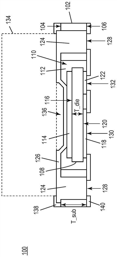
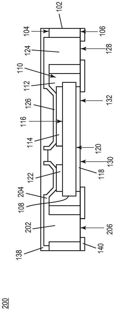
[0122] Example 1. A semiconductor package comprising: an insulating substrate having a first main side and a second main side opposite the first main side; a power semiconductor die embedded in the insulating substrate and compared The insulating substrate is thin or as thick as the insulating substrate, the power semiconductor die comprising a first load terminal on a first side facing in the same direction as the first main side of the insulating substrate Bonding pads, second load terminal bonding pads at the second side facing the same direction as the second main side of the insulating substrate, and control terminal bonding pads at the first side or the second side Plate; Conductive first via, which extends through the insulating substrate in a peripheral region laterally surrounding the power semiconductor die; first metallization, which connects the power semiconductor die at the first main side of the insulating substrate A first load terminal bonding pad connected to...
example 2
[0123] Example 2. The semiconductor package of example 1, wherein the control terminal bond pad is at the second side of the power semiconductor die, the semiconductor package further comprising: a solderable third contact pad, It is at the second main side of the insulating substrate and is formed by control terminal bond pads of the power semiconductor die.
example 3
[0124] Example 3. The semiconductor package of example 1, wherein the control terminal bond pad is at the first side of the power semiconductor die, the semiconductor package further comprising: a conductive second via at extending through the insulating substrate in the peripheral region; a second metallization connecting a control terminal bond pad of the power semiconductor die to a second via at the first main side of the insulating substrate; and A solderable third contact pad at the second main side of the insulating substrate and formed by the second via.
PUM
| Property | Measurement | Unit |
|---|---|---|
| Thickness | aaaaa | aaaaa |
Abstract
Description
Claims
Application Information
 - R&D
- Intellectual Property
- Life Sciences
- Materials
- Tech Scout
- Unparalleled Data Quality
- Higher Quality Content
- 60% Fewer Hallucinations
Browse by: Latest US Patents, China's latest patents, Technical Efficacy Thesaurus, Application Domain, Technology Topic, Popular Technical Reports.
© 2025 PatSnap. All rights reserved.Legal|Privacy policy|Modern Slavery Act Transparency Statement|Sitemap|About US| Contact US: help@patsnap.com


