Substrate chuck for self-assembling semiconductor light emitting diodes

A substrate card and substrate technology, which is applied in semiconductor devices, semiconductor/solid-state device manufacturing, electric solid-state devices, etc., can solve the problems of insufficient research on displays, etc., and achieve the effects of easy loading or unloading, fast transfer, and low cost

Active Publication Date: 2021-08-17
LG ELECTRONICS INC
View PDF10 Cites 0 Cited by
  • Summary
  • Abstract
  • Description
  • Claims
  • Application Information

AI Technical Summary

Problems solved by technology

[0005] Recently, U.S. Patent Registration No. 9,825,202 discloses a micro-LED structure suitable for self-assembly, but the technology for manufacturing displays by self-assembly of micro-LEDs is understudied

Method used


Image

  • Substrate chuck for self-assembling semiconductor light emitting diodes
  • Substrate chuck for self-assembling semiconductor light emitting diodes
  • Substrate chuck for self-assembling semiconductor light emitting diodes

Examples


Embodiment Construction

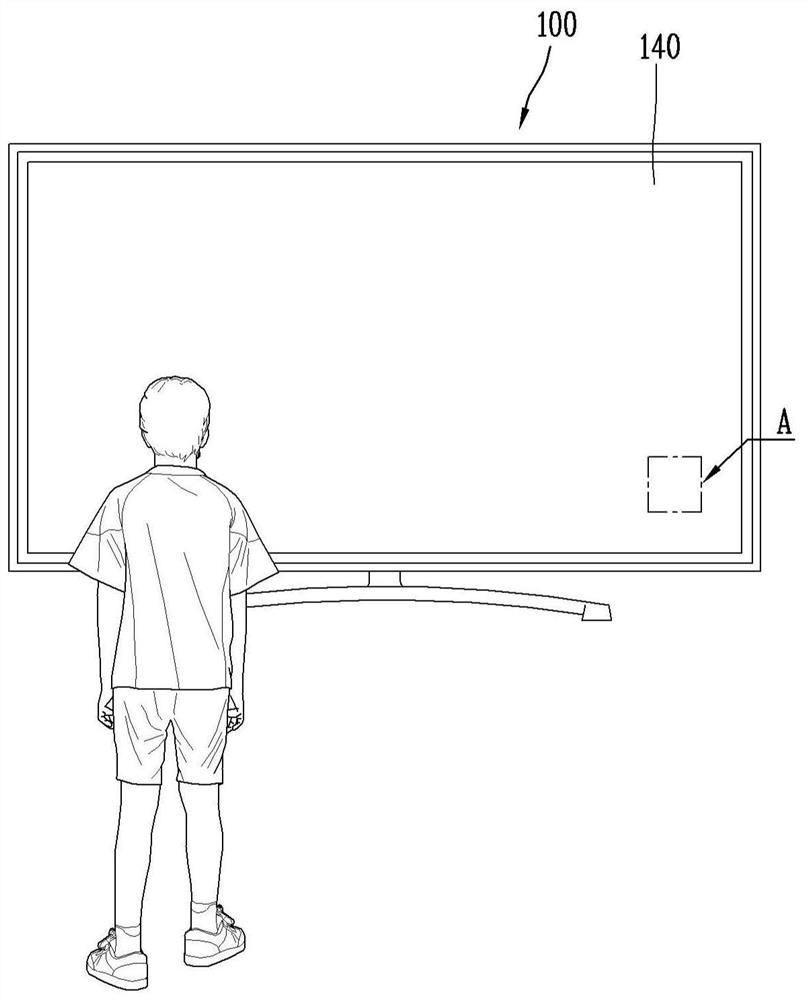
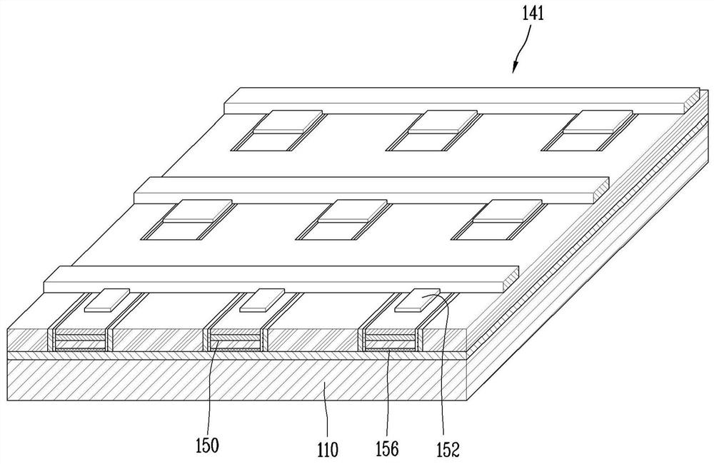
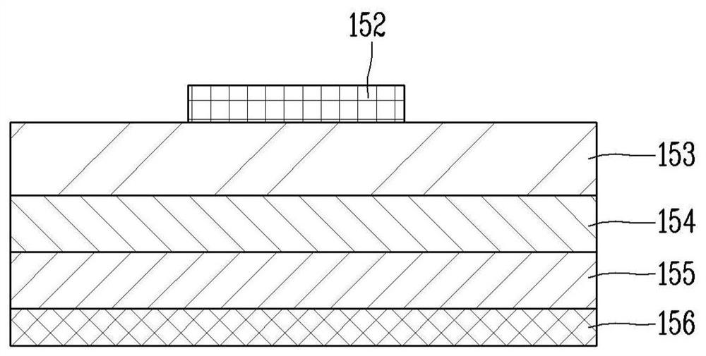
[0056]Description will now be given in detail according to the exemplary embodiments disclosed herein with reference to the accompanying drawings. For the sake of brief description with reference to the drawings, the same or equivalent components may be given the same or similar reference numerals, and description thereof will not be repeated. Generally, suffixes such as "module" and "unit" may be used to refer to elements or components. The use of such suffixes herein is only intended to facilitate the description of the specification, and the suffixes themselves are not intended to give any special meaning or function. In describing the present disclosure, if a detailed explanation for a related known function or construction is considered to unnecessarily divert the gist of the present disclosure, such explanation has been omitted but will be understood by those skilled in the art. The accompanying drawings are used to help easily understand the technical idea of ​​the pre...


PUM


Abstract

The present disclosure relates to a method for manufacturing a display device, and one particular implementation relates to a substrate chuck for self-assembling micro LEDs. The substrate chuck may include a first frame having a hole at a central portion thereof, a second frame having a hole at a central portion thereof and disposed to overlap the first frame, a frame moving part configured to transfer the second frame such that the second frame presses the substrate while the substrate is disposed between the first and second frames, and an auxiliary clamp configured to additionally press the second frame toward the substrate while the second frame is pressing the substrate.

Description

technical field [0001] The present disclosure relates to a method for manufacturing a display device, and one particular embodiment relates to a substrate chuck for self-assembling micro-LEDs. Background technique [0002] In recent years, in the field of display technologies, liquid crystal displays (LCDs), organic light emitting diode (OLED) displays, micro LED (microLED) displays, and the like have been competing to realize large-area displays. [0003] In contrast, when semiconductor microLEDs (μLEDs) with a diameter or cross-sectional area of ​​less than 100 micrometers are used in displays, they can deliver very high efficiencies because the displays do not require polarizers to absorb light. However, large displays require millions of semiconductor light-emitting diodes, which makes transferring the devices difficult compared to other technologies. [0004] Some of the technologies currently being developed for transfer processes include pick-and-place, laser lift-of...

Claims


Application Information

Patent Timeline
Patent Type & Authority Applications(China)
IPC IPC(8): H01L21/687H01L21/67H01L33/48
CPCH01L21/67288H01L21/68785H01L21/67253H01L33/48H01L2933/0033H01L21/67346H01L21/6831H01L21/68735H01L21/68742H01L21/6875H01L21/68714H01L21/687H01L2224/95101H01L21/68728H01L21/67144B25B5/02H01L21/68778H01L25/13
Inventor 杨仁范郑任悳鲁正勋崔凤云
Owner LG ELECTRONICS INC
Why Eureka
Try Eureka