PCB impedance control method, device and equipment and readable storage medium

A technology of impedance control and control, which is applied in the secondary processing of printed circuits, electrical components, and printed circuit manufacturing, etc. It can solve problems affecting PCB impedance matching, uneven solder mask thickness, and affecting impedance values, etc.

Pending Publication Date: 2021-08-20
LANGCHAO ELECTRONIC INFORMATION IND CO LTD
View PDF9 Cites 0 Cited by
  • Summary
  • Abstract
  • Description
  • Claims
  • Application Information

AI Technical Summary

Problems solved by technology

However, due to the presence of signal traces in some areas on the surface of the PCB, the thickness of the solder mask in different areas on the processed PCB will be uneven, and the thickness of the solder mask will affect the impedance value, which in turn affects the impedance matching of the PCB, resulting in uneven solder mask thickness on the PCB. The signal integrity of the signal line is not guaranteed, especially the signal from the central processing unit (CPU) to the small dual in-line memory module (Small Outline Dual In-line Memory Module, SODIMM) line part

Method used


Image

  • PCB impedance control method, device and equipment and readable storage medium
  • PCB impedance control method, device and equipment and readable storage medium
  • PCB impedance control method, device and equipment and readable storage medium

Examples


Embodiment 1

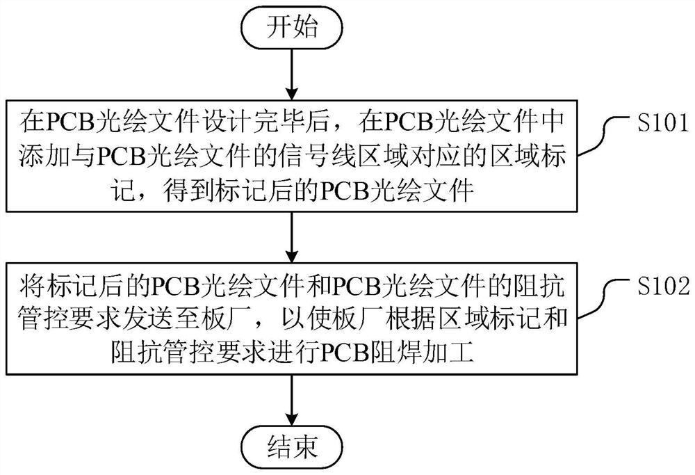
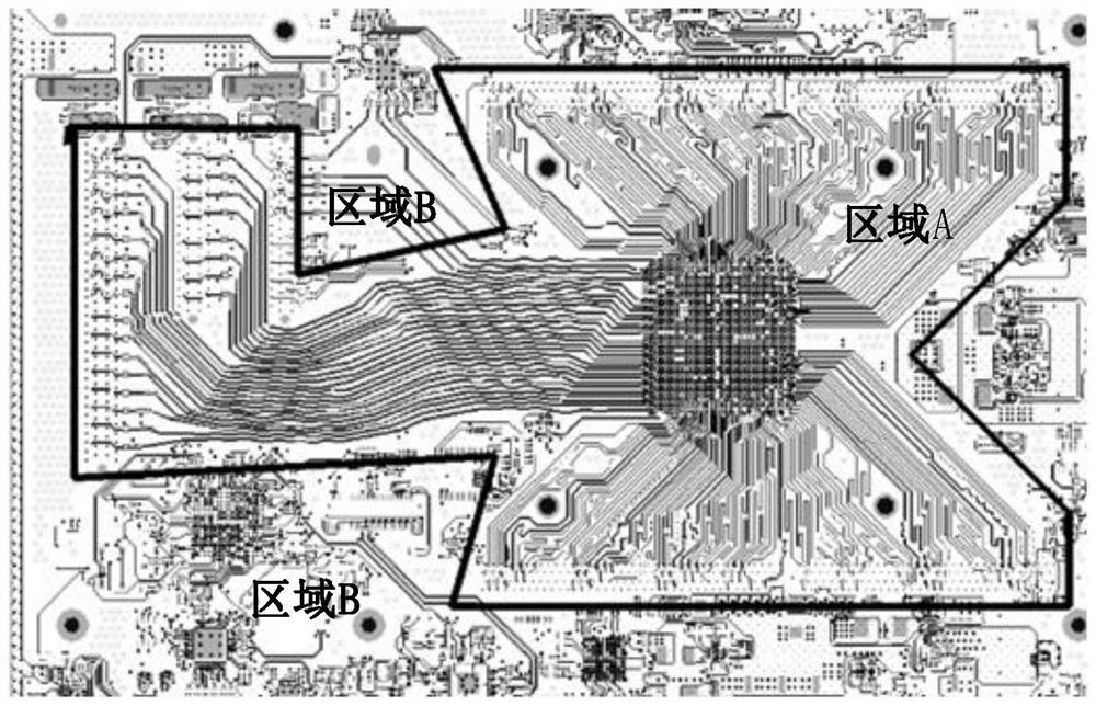
[0044] figure 1 A flow chart of the first PCB impedance control method provided in the embodiment of the present application; figure 2 It is a schematic diagram of a marked PCB gerber file provided in the embodiment of this application.

[0045] like figure 1 As shown, the method for PCB impedance control provided by the embodiment of the present application includes:

[0046] S101: After the design of the PCB light-drawing file is completed, an area mark corresponding to the signal line area of ​​the PCB light-drawing file is added to the PCB light-drawing file to obtain a marked PCB light-drawing file.

[0047] S102: Send the marked PCB light drawing file and the impedance control requirements of the PCB light drawing file to the board factory, so that the board factory performs PCB solder mask processing according to the area marking and impedance control requirements.

[0048] Impedance matching is mainly used on transmission lines to achieve the purpose that all high-...

Embodiment 2

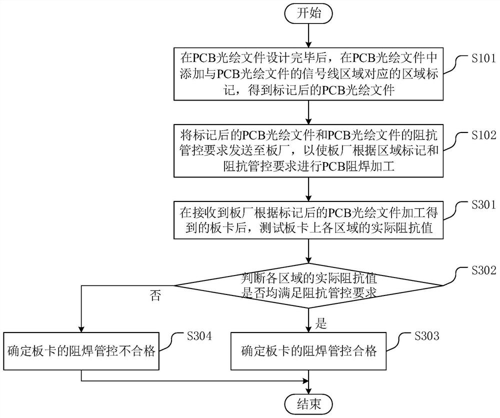
[0057] image 3 A flowchart of another PCB impedance control method provided by the embodiment of the present application; Figure 4 It is a schematic diagram of an impedance test principle provided in the embodiment of the present application.

[0058] On the basis of the above examples, if image 3 As shown, the method for PCB impedance control provided by the embodiment of the present application includes:

[0059] S101: After the design of the PCB light-drawing file is completed, an area mark corresponding to the signal line area of ​​the PCB light-drawing file is added to the PCB light-drawing file to obtain a marked PCB light-drawing file.

[0060] S102: Send the marked PCB light drawing file and the impedance control requirements of the PCB light drawing file to the board factory, so that the board factory performs PCB solder mask processing according to the area marking and impedance control requirements.

[0061] S301: After receiving the board processed by the boa...

Embodiment 3

[0072] Figure 5 It is a flow chart of the third PCB impedance control method provided by the embodiment of this application.

[0073] On the basis of the above examples, if Figure 5 As shown, the method for PCB impedance control provided by the embodiment of the present application includes:

[0074] S101: After the design of the PCB light-drawing file is completed, an area mark corresponding to the signal line area of ​​the PCB light-drawing file is added to the PCB light-drawing file to obtain a marked PCB light-drawing file.

[0075] S102: Send the marked PCB light drawing file and the impedance control requirements of the PCB light drawing file to the board factory, so that the board factory performs PCB solder mask processing according to the area marking and impedance control requirements.

[0076] S301: After receiving the board processed by the board factory according to the marked PCB photo-painting file, test the actual impedance value of each area on the board. ...


PUM


Abstract

The invention discloses a PCB impedance control method. The method comprises the steps: adding a region mark corresponding to a signal line region of a PCB light painting file in the PCB light painting file after the design of the PCB light painting file is completed, obtaining a marked PCB light painting file, and then transmitting the marked PCB light painting file and an impedance control requirement of the PCB light painting file to a board factory. Therefore, when the board factory carries out PCB resistance welding processing, distinguishing processing can be carried out according to the region mark and impedance control requirement, and the problem that the signal integrity cannot be guaranteed due to unqualified impedance matching caused by uneven resistance welding thickness of a signal line area due to the fact that the board factory processes the PCB according to a unified standard is solved. The invention further discloses a PCB impedance control device and equipment and a readable storage medium, which have the above beneficial effects.

Description

technical field [0001] The present application relates to the technical field of PCB, in particular to a method, device, equipment and readable storage medium for PCB impedance control. Background technique [0002] In order to avoid oxidation of the copper foil on the surface (usually including the top and bottom layers) of printed circuit boards (Printed circuit boards, also known as printed circuit boards, hereinafter referred to as PCB), existing PCBs usually add solder mask to the surface layer, That is green oil. However, due to the presence of signal traces in some areas on the surface of the PCB, the thickness of the solder mask in different areas on the processed PCB will be uneven, and the thickness of the solder mask will affect the impedance value, which in turn will affect the impedance matching of the PCB, resulting in uneven solder mask thickness on the PCB. The signal integrity of the signal line is not guaranteed, especially the signal from the central proc...

Claims


Application Information

Patent Timeline
Patent Type & Authority Applications(China)
IPC IPC(8): H05K3/28
CPCH05K3/282
Inventor 孙广元
Owner LANGCHAO ELECTRONIC INFORMATION IND CO LTD
Why Eureka
Try Eureka