Mask plate, semiconductor device and method for manufacturing semiconductor device

A manufacturing method and a technology of mask plates, which are applied in the field of mask plates, can solve problems such as insufficient space and inability to place test component groups, and achieve the effect of improving yield

Active Publication Date: 2022-03-04
CHANGXIN MEMORY TECH INC
View PDF8 Cites 0 Cited by
  • Summary
  • Abstract
  • Description
  • Claims
  • Application Information

AI Technical Summary

Problems solved by technology

[0006] The present invention provides a mask plate, a semiconductor device, and a method for manufacturing a semiconductor device, so as to solve the problem in the above-mentioned related art that there is insufficient space in the exposure range and two groups of adjacent test element groups cannot be placed

Method used


Image

  • Mask plate, semiconductor device and method for manufacturing semiconductor device
  • Mask plate, semiconductor device and method for manufacturing semiconductor device
  • Mask plate, semiconductor device and method for manufacturing semiconductor device

Examples


Embodiment Construction

[0059] Example embodiments will now be described more fully with reference to the accompanying drawings. Example embodiments may, however, be embodied in many forms and should not be construed as limited to the embodiments set forth herein; rather, these embodiments are provided so that this disclosure will be thorough and complete, and will fully convey the concept of example embodiments to those skilled in the art. The same reference numerals in the drawings denote the same or similar structures, and thus their detailed descriptions will be omitted.

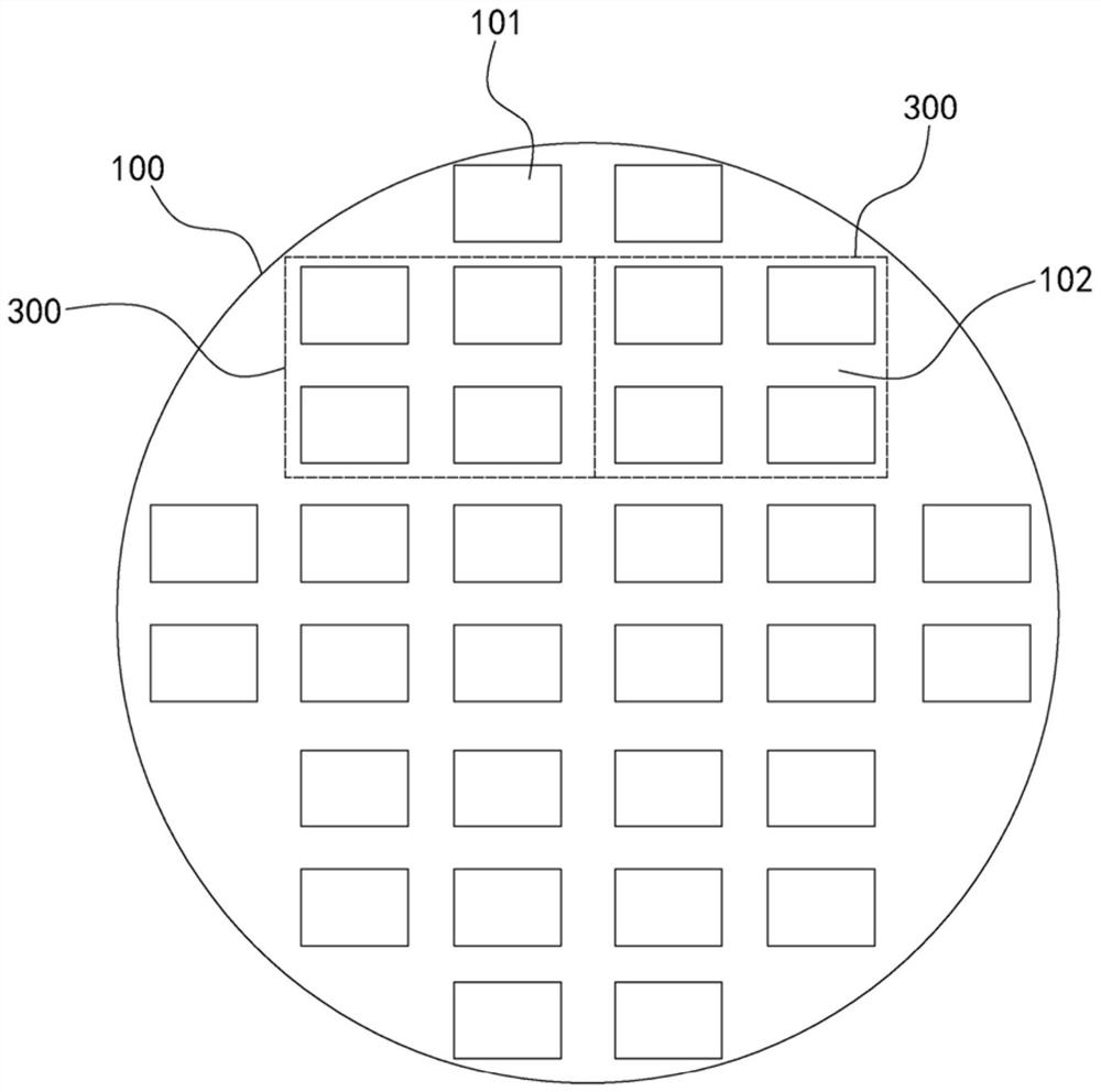
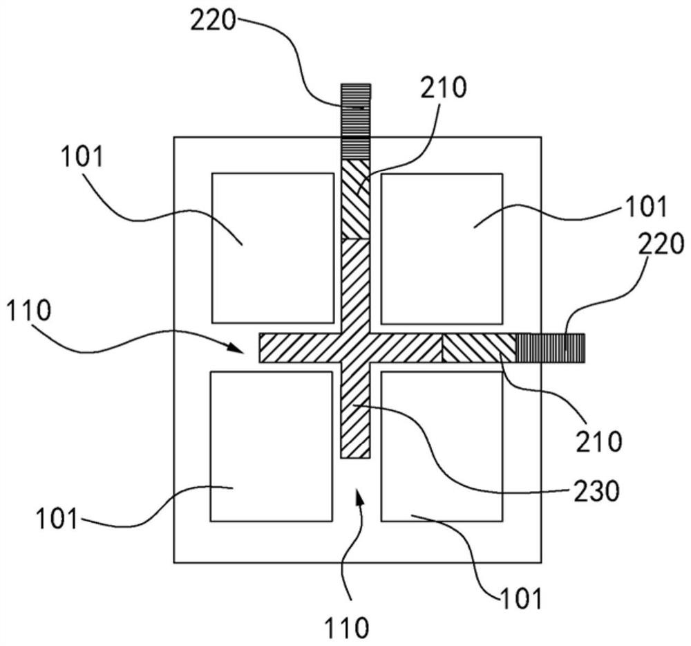
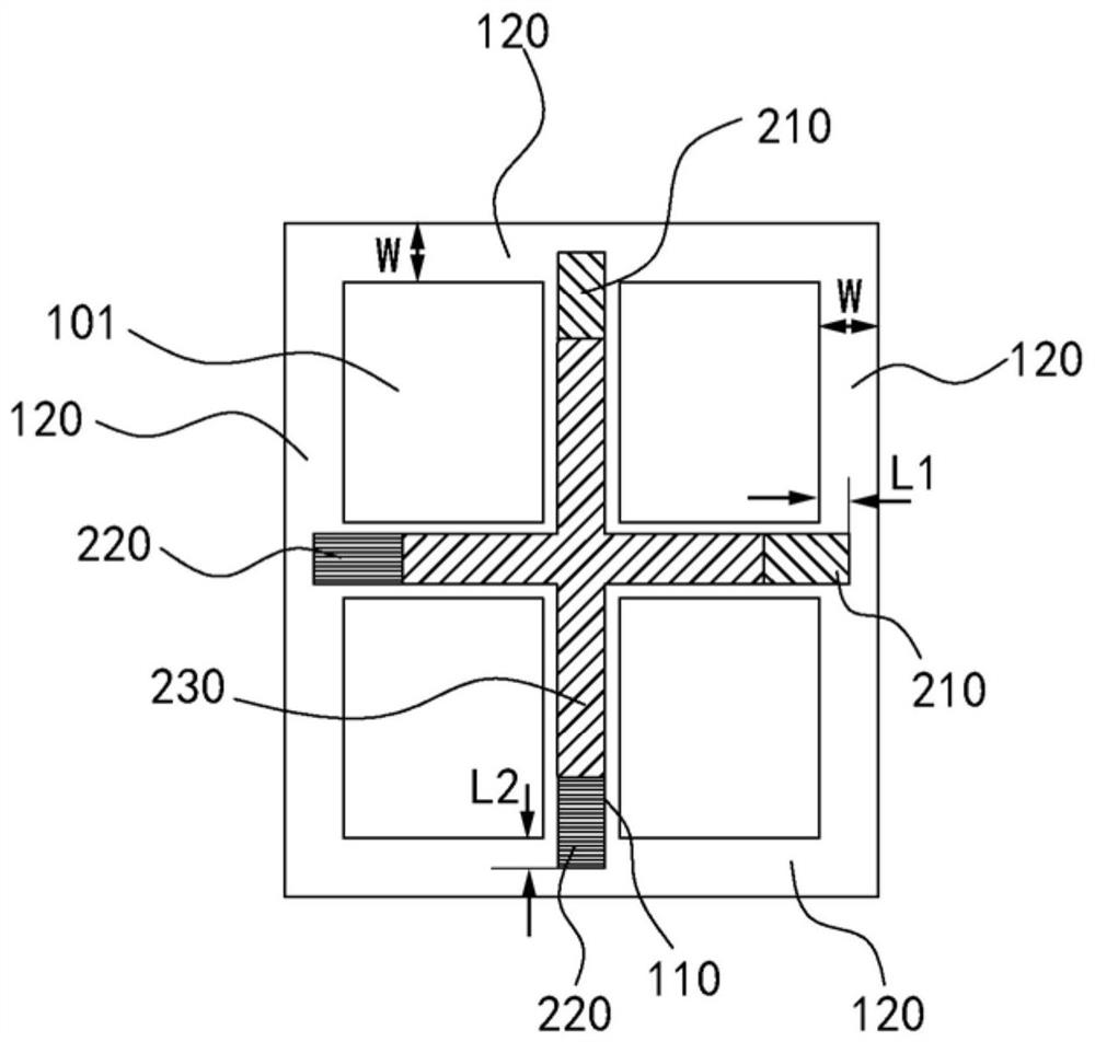
[0060] Such as figure 1 as shown, figure 1 A plan view of a semiconductor device is shown. The semiconductor device includes a plurality of integrated circuit regions 101 and dicing regions 102 . Integrated circuits are integrated in the integrated circuit area 101 , and the cutting area 102 is arranged between every two adjacent integrated circuit areas 101 . The cutting area 102 is used as a space for a dicing blade to m...


PUM


Abstract

The invention relates to a mask plate, a semiconductor device and a method for manufacturing the semiconductor device. The mask plate is used to form a pattern on a wafer through exposure, including a scribe pattern, a first pattern and a second pattern. The scribe pattern is used for The dicing region of the wafer forms dicing streets, and the dicing street pattern includes oppositely disposed first and second ends. The first pattern is located at the first end and is used to form a first test element group pattern in the dicing line. The second pattern is located at the second end and spaced apart from the first pattern for forming a second test element group pattern in the cutting line. Wherein, when a plurality of exposure patterns exposed by mask plates are formed on the wafer, the first test element group pattern of one of the two adjacent exposure patterns and the second test element group pattern of the other exposure pattern Set of patterns adjoining.

Description

technical field [0001] The present invention relates to the technical field of semiconductors, in particular to a mask plate, a semiconductor device and a method for manufacturing the semiconductor device. Background technique [0002] At present, the manufacturing process of semiconductor chips can be roughly divided into two parts: the wafer preparation process and the assembly and testing process. The wafer preparation process involves preparing a semiconductor wafer containing multiple integrated circuits, and the assembly and testing process involves processing the semiconductor wafer into a desired form of semiconductor product. [0003] Typically, dicing is a step in the assembly and testing process that involves dicing a semiconductor wafer containing multiple identical integrated circuits into individual semiconductor chips. Specifically, dicing is performed by cutting a semiconductor wafer with a dicing blade. The area where the semiconductor wafer is cut by the ...

Claims


Application Information

Patent Timeline
Patent Type & Authority Patents(China)
IPC IPC(8): G03F1/00G03F1/38
CPCG03F1/00G03F1/38
Inventor 李静
Owner CHANGXIN MEMORY TECH INC
Why Eureka
Try Eureka