Infrared measuring device
A measuring device, infrared technology, applied in the direction of optical device exploration, etc., can solve the problem of rising device cost and so on
- Summary
- Abstract
- Description
- Claims
- Application Information
AI Technical Summary
Problems solved by technology
Method used
Image
Examples
Deformed example 1
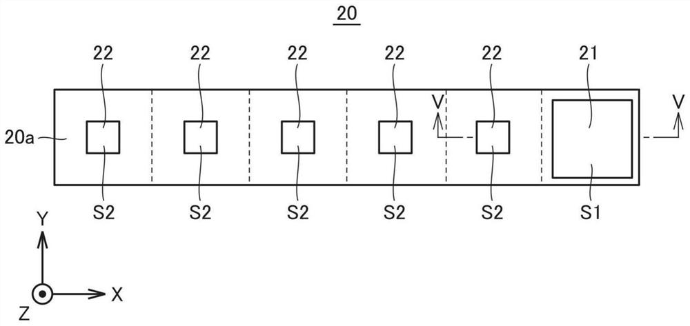
[0065] In the above-mentioned embodiment, the size of the P layer 33b and the N layer 34b arranged in each visible light receiving part 22 is smaller than the size of the P layer 33a and N layer 34a arranged in the infrared light receiving part 21, so that each visible light receiving part The example in which the light-receiving area S2 of the infrared light-receiving part 21 is smaller than the light-receiving area S1 of the infrared light-receiving part 21 has been described (see above figure 2 as well as Figure 5 ).
[0066] However, the method of making the light receiving area S2 of each visible light receiving section 22 smaller than the light receiving area S1 of the infrared light receiving section 21 is not limited to the above method.
[0067] Figure 11 It is a figure which looked at the light receiving part 20A of this modification 1 from the Z-axis direction. In this light receiving part 20A, by making the size of the P layer 33a and the N layer 34a arranged...
Deformed example 2
[0069] In the above-mentioned embodiment, an example was shown in which the light-receiving areas of the plurality of visible light-receiving parts 22 were substantially equal to each other (see the above-mentioned figure 2 ), however, the light receiving areas of the plurality of visible light receiving units 22 may be different from each other.
[0070] Figure 12 It is a figure which looked at the light receiving part 20B of this modification 2 from the Z-axis direction. In this light receiving unit 20B, the light receiving areas of the plurality of visible light receiving units 22B1 to 22B5 are all smaller than the light receiving area S1 of the infrared light receiving unit 21 and are different from each other. In this way, the light receiving areas of the plurality of visible light receiving units 22B1 to 22B5 may also be made different from each other.
Deformed example 3
[0072] In the above embodiment, an example in which the infrared light receiving unit 21 and the plurality of visible light receiving units 22 are arranged in a straight line has been shown (see the above-mentioned figure 2 ), but the arrangement of the infrared light receiving unit 21 and the plurality of visible light receiving units 22 is not limited to a straight line.
[0073] Figure 13 It is a figure which looked at 20 C of light receiving parts of this modification 3 from the Z-axis direction. In this light receiving unit 20C, a plurality (eight) of visible light receiving units 22 are arranged in a ring shape with the infrared light receiving unit 21 at the center. By deforming in this manner, it is possible to arrange a plurality of visible light receiving units 22 at positions close to the infrared receiving unit 21 .
PUM
 Abstract
Description
Claims
Application Information


