A Microstrip Slow-wave Structure Transmission System Suitable for Wide Dielectric Substrate

A medium-substrate, slow-wave structure technology, used in waveguides, waveguide-type devices, circuit components of transit-time electron tubes, etc. problems, to achieve the effect of improving transmission performance, filtering out waveguide modes, and overcoming reflections

Active Publication Date: 2022-04-15
UNIV OF ELECTRONICS SCI & TECH OF CHINA
View PDF5 Cites 0 Cited by
  • Summary
  • Abstract
  • Description
  • Claims
  • Application Information

AI Technical Summary

Problems solved by technology

However, when the lateral width of the dielectric substrate is wide, it will be difficult to achieve a good match between the microstrip slow-wave structure and the input and output waveguides, resulting in that part of the microwave is not converted into the quasi-TEM mode required for microstrip propagation after being input from the waveguide, but is still in the waveguide mode. Propagate in the slow wave structure, which leads to large reflection and poor transmission performance of the microstrip slow wave transmission system, which will affect the normal operation of the slow wave structure

Method used


Image

  • A Microstrip Slow-wave Structure Transmission System Suitable for Wide Dielectric Substrate
  • A Microstrip Slow-wave Structure Transmission System Suitable for Wide Dielectric Substrate
  • A Microstrip Slow-wave Structure Transmission System Suitable for Wide Dielectric Substrate

Examples


Embodiment

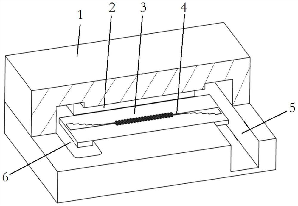
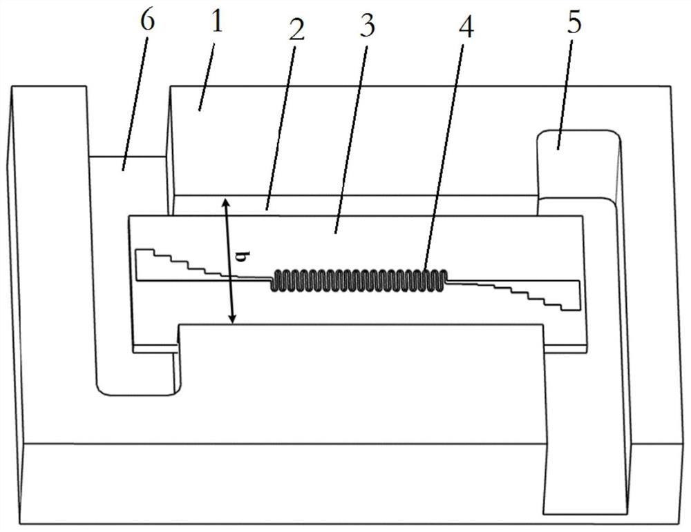
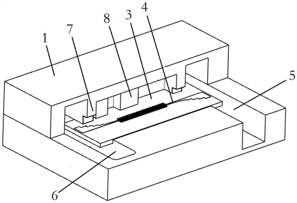
[0038] Embodiment: a kind of microstrip slow-wave structure transmission system suitable for wide dielectric substrate 3, such as image 3 and Figure 4 As shown, it includes a metal casing 1 and a dielectric substrate 3 provided with a microstrip slow wave line 4. The metal casing 1 is provided with a vacuum cavity 2, an input waveguide 5, and an output waveguide 6. The dielectric substrate 3 is installed in the vacuum cavity 2, and The two ends of the dielectric substrate 3 are respectively placed in the input waveguide 5 and the output waveguide 6, and the side wall of the vacuum chamber 2 is provided with two sets of first protrusions 7 and two sets of second protrusions 8, two sets of first protrusions 7 and two sets of The second protrusions 8 are all located on the side of the dielectric substrate 3 where the microstrip slow wave line 4 is disposed. Two groups of first protrusions 7 and two groups of second protrusions 8 are arranged at intervals along the microwave pr...


PUM


Abstract

The invention discloses a microstrip slow-wave structure transmission system suitable for wide dielectric substrates, and relates to the field of microwave electric vacuum technology. Protrusions, two groups of first protrusions and two groups of second protrusions are located on the side of the microstrip slow wave line in the dielectric substrate; two groups of first protrusions and two groups of second protrusions are located along the microstrip slow wave line The microwave propagating direction of the line is arranged at intervals, and two groups of second protrusions are located between two groups of first protrusions; the lateral width of the first protrusions is greater than that of the second protrusions. The present invention changes the shape of the inner wall of the metal shell innovatively, so that the cut-off frequency of microwave propagation in multiple places changes suddenly, that is, a new capacitive reactance and inductive reactance are introduced into the slow wave structure, so as to filter out the waveguide mode and improve the efficiency of the slow wave structure. The role of transmission performance effectively overcomes the problem of large reflection and transmission loss when the wide dielectric substrate microstrip slow-wave structure transmits microwave signals.

Description

technical field [0001] The invention relates to the field of microwave electric vacuum technology, more specifically, it relates to a microstrip slow-wave structure transmission system suitable for wide dielectric substrates. Background technique [0002] Microwave electric vacuum device refers to an electronic system that uses the movement of charged particles between electrodes to realize the oscillation or amplification of microwave signals in a vacuum state. It has the advantages of high power, high frequency, radiation resistance, and strong environmental adaptability. It is used in many fields of national defense weaponry and national economy. [0003] Currently, traveling wave tubes are one of the most widely used power amplifiers in microwave vacuum electronics. As the core place where the electron beam and the microwave interact with each other in the TWT, the performance of the slow-wave structure greatly affects the working performance of the TWT. The traditiona...

Claims


Application Information

Patent Timeline
Patent Type & Authority Patents(China)
IPC IPC(8): H01J23/24H01P3/10
CPCH01J23/24H01P3/10
Inventor 岳玲娜刘驰艺芦佳王文祥陈冬春徐进殷海荣赵国庆魏彦玉
Owner UNIV OF ELECTRONICS SCI & TECH OF CHINA
Why Eureka
Try Eureka