Nonvolatile memory circuit, and storage method and reading method thereof

A non-volatile memory and circuit technology, applied in information storage, static memory, digital memory information and other directions, can solve the problems of poor memory performance, complex memory circuits, and many devices

Pending Publication Date: 2021-09-07
SEMICON MFG INT (SHANGHAI) CORP +1
View PDF6 Cites 0 Cited by
  • Summary
  • Abstract
  • Description
  • Claims
  • Application Information

AI Technical Summary

Problems solved by technology

[0004] However, the existing memory circuits are relatively complex, there are many devices, and the performance of the memory is poor

Method used


Image

  • Nonvolatile memory circuit, and storage method and reading method thereof
  • Nonvolatile memory circuit, and storage method and reading method thereof
  • Nonvolatile memory circuit, and storage method and reading method thereof

Examples


Embodiment Construction

[0025] As described in the background, existing memory circuits are relatively complex and have many devices, resulting in high cost and poor performance of the memory.

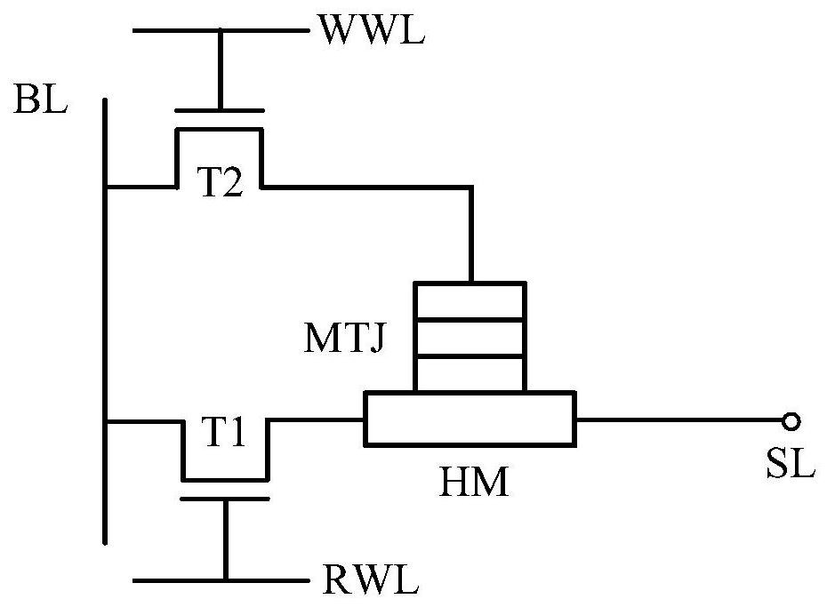
[0026] figure 1 It is a schematic diagram of the circuit structure of a non-volatile storage circuit.

[0027] Please refer to figure 1 , the non-volatile storage circuit includes: a first word line RWL, a second word line WWL, a first bit line BL, a source line SL, a magnetic storage unit, a first transistor T1 and a second transistor T2.

[0028] The magnetic memory unit includes: a Hall effect layer HM and a magnetic tunnel junction MTJ located on the surface of the Hall effect layer, and the Hall effect layer HM has a first end and a second end.

[0029] The second terminal of the Hall effect layer HM is coupled to the source line SL.

[0030] The drain of the first transistor T1 is coupled to the first end of the Hall effect layer HM, the gate of the first transistor T1 is coupled to the first word li...


PUM


Abstract

The invention discloses a nonvolatile memory circuit and a storage method and a reading method thereof; the nonvolatile memory circuit comprises: a spin-orbit momentum magnetic memory, wherein the spin-orbit momentum magnetic memory comprises a spin Hall effect layer, a first magnetic tunnel junction and a second magnetic tunnel junction, the spin Hall effect layer is provided with a first surface and a second surface which are opposite to each other, the first magnetic tunnel junction is positioned on the first surface, the second magnetic tunnel junction is positioned on the second surface, and the spin Hall effect layer further comprises a first end and a second end; a first bit line; a second bit line; a third bit line; a fourth bit line; and a switch assembly that couples the first end with the first bit line, couples the second end with the second bit line, and couples the first magnetic tunnel junction with the third bit line, and couples the second magnetic tunnel junction with the fourth bit line. Therefore, the cost of the memory is reduced, and the performance of the memory is improved.

Description

technical field [0001] The present invention relates to the technical field of integrated circuits, in particular to a non-volatile storage circuit, a storage method and a reading method thereof. Background technique [0002] Memory is widely used in a variety of electronic devices, such as cellular telephones, digital cameras, personal digital assistants, medical electronics, mobile computing devices, non-mobile computing devices, and data servers. Memory can include non-volatile memory or volatile memory. [0003] Non-volatile memory includes magnetic memory (MRAM), among others, which allows information to be stored and retained when not connected to a power source, in contrast to volatile memory. [0004] However, the existing memory circuits are relatively complex, have many devices, and the performance of the memory is poor. Contents of the invention [0005] The technical problem solved by the present invention is to provide a non-volatile memory circuit and its s...

Claims


Application Information

Patent Timeline
Patent Type & Authority Applications(China)
IPC IPC(8): G11C11/16G11C11/18
CPCG11C11/161G11C11/1655G11C11/1657G11C11/1673G11C11/1675G11C11/18
Inventor 刘盼盼张海洋
Owner SEMICON MFG INT (SHANGHAI) CORP
Why Eureka
Try Eureka