A display panel and its preparation method, silicon-based organic light-emitting microdisplay

A technology for display panels and organic light-emitting layers, which is applied in semiconductor devices, electric solid-state devices, and semiconductor/solid-state device manufacturing. The effect of leaking flow and ensuring continuity

Active Publication Date: 2022-06-03
KUNSHAN FANTAVIEW ELECTRONICS TECH CO LTD
View PDF5 Cites 0 Cited by
  • Summary
  • Abstract
  • Description
  • Claims
  • Application Information

AI Technical Summary

Problems solved by technology

The method of reducing the proportion of hole-injecting materials is less accurate and cannot completely solve the problem of lateral leakage

Method used


Image

  • A display panel and its preparation method, silicon-based organic light-emitting microdisplay
  • A display panel and its preparation method, silicon-based organic light-emitting microdisplay
  • A display panel and its preparation method, silicon-based organic light-emitting microdisplay

Examples


Embodiment Construction

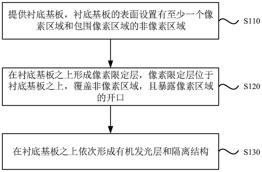
[0038] The present invention will be further described in detail below in conjunction with the accompanying drawings and embodiments. It should be understood that the specific embodiments described here are only used to explain the present invention, but not to limit the present invention. In addition, it should be noted that, for the convenience of description, only some structures related to the present invention are shown in the drawings but not all structures.

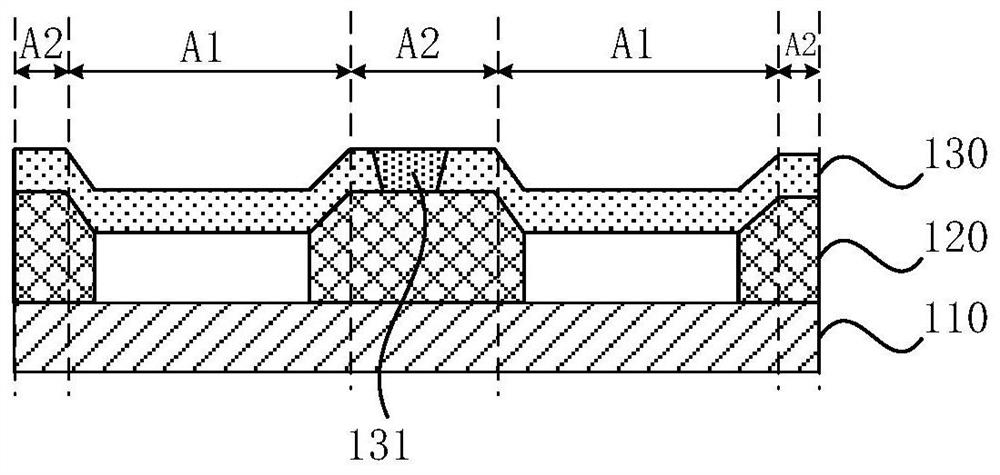
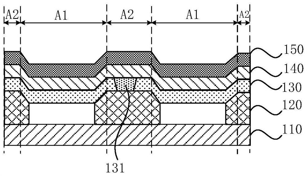
[0039] figure 1 is a schematic structural diagram of a display panel provided by an embodiment of the present invention, see figure 1 , the display panel includes: a base substrate 110, the surface of the base substrate 110 is provided with at least one pixel area A1 and a non-pixel area A2 surrounding the pixel area; a pixel defining layer 120, the pixel defining layer 120 is located on the base substrate 110, Covering the non-pixel area A2 and exposing the opening of the pixel area A1; the organic light-emittin...


PUM


Abstract

The invention discloses a display panel, a preparation method thereof, and a silicon-based organic light-emitting microdisplay. The display panel includes a base substrate, the surface of the base substrate is provided with at least one pixel area and a non-pixel area surrounding the pixel area; a pixel definition layer, the pixel definition layer is located on the base substrate, covers the non-pixel area, and exposes the pixel area The opening of the organic light-emitting layer and the isolation structure, the organic light-emitting layer and the isolation structure are located on the base substrate, wherein the organic light-emitting layer is located in the pixel area, and the isolation structure is located on the surface of the pixel definition layer away from the base substrate, and is located on the non-pixel area, the surface of the isolation structure away from the base substrate is a plane. The present invention achieves the effect of accurately disconnecting the continuity of the non-pixel region in the light-emitting machine layer.

Description

technical field [0001] The embodiments of the present invention relate to the field of display technology, in particular to a display panel, a manufacturing method thereof, and a silicon-based organic light-emitting microdisplay. Background technique [0002] Existing organic light-emitting display panels, such as silicon-based organic light-emitting display panels, have a very small pixel pitch, because organic materials themselves are semiconductors and have certain charge transfer capabilities, especially hole injection materials. It is very small, and silicon-based micro-displays are vapor-deposited on a common mask, and the material has good continuity. Therefore, when one of the pixels is lit, part of the current is more likely to leak to adjacent pixels, and the It causes adjacent pixels to emit light slightly, which is the so-called crosstalk. Pixel crosstalk will cause the color coordinates to shift after lighting, and the color purity is poor. In severe cases, it c...

Claims


Application Information

Patent Timeline
Patent Type & Authority Patents(China)
IPC IPC(8): H01L51/52H01L51/56H01L27/32
CPCH10K59/12H10K50/8428H10K59/1201H10K71/00
Inventor 王卫卫周文斌朱晓庆沈倩徐超陆炎孙剑高裕弟
Owner KUNSHAN FANTAVIEW ELECTRONICS TECH CO LTD
Why Eureka
Try Eureka