

Substrate treatment method and substrate treatment device
A substrate processing method and substrate technology, which can be used in electrical components, semiconductor/solid-state device manufacturing, circuits, etc., and can solve problems such as poor etching
- Summary
- Abstract
- Description
- Claims
- Application Information
AI Technical Summary
Problems solved by technology
Method used
Image

Examples
Embodiment Construction
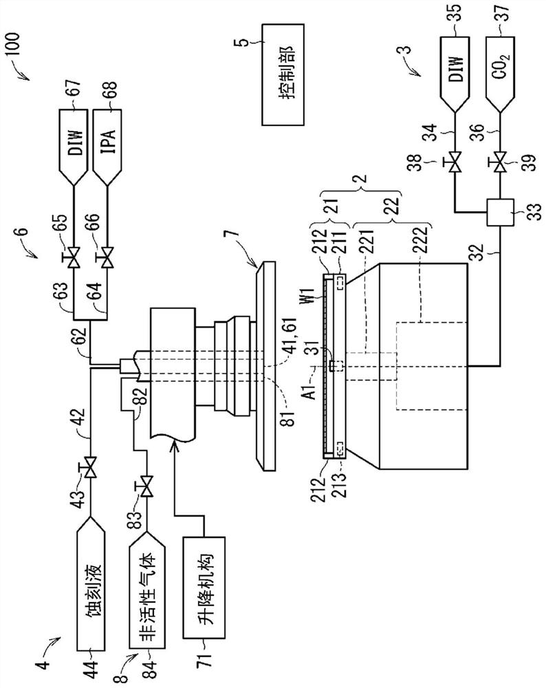
[0047] Below, refer to the attached Figure 1 Embodiments will be described. In addition, the drawings are diagrams schematically shown, and for convenience of description, the configuration is appropriately omitted or simplified. In addition, the relationship between the size and position of the configuration shown in the drawings is not necessarily described accurately, and can be appropriately changed.
[0048] In addition, in the description shown below, the same reference numerals are assigned to the same components and shown, and their names and functions are also set to be the same. Therefore, there are cases where detailed descriptions thereof are omitted to avoid repetition.
[0049]
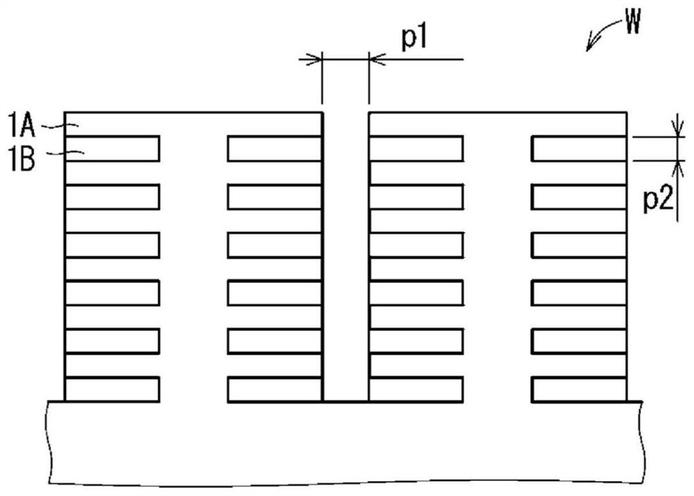
[0050] figure 1 It is a diagram schematically showing an example of the configuration of the substrate processing apparatus 100 . The substrate processing apparatus 100 supplies an etchant to the surface of the substrate W1 to etch the surface of the substrate W1. The substrate W1...
PUM
 Abstract
Description
Claims
Application Information