Hadamard product implementation method and device and storage medium

A realization method, Hada technology, applied in the field of optoelectronic chips

Active Publication Date: 2021-09-14
INSPUR SUZHOU INTELLIGENT TECH CO LTD
View PDF2 Cites 2 Cited by
  • Summary
  • Abstract
  • Description
  • Claims
  • Application Information

AI Technical Summary

Problems solved by technology

[0003] Today's most common industrial solution for Optical Neural Network (ONN) is to set up proprietary devices, but it is generally only suitable for solving the multiplication and addition operations based on convolution operations

Method used


Image

  • Hadamard product implementation method and device and storage medium
  • Hadamard product implementation method and device and storage medium
  • Hadamard product implementation method and device and storage medium

Examples


Embodiment Construction

[0032] The following will clearly and completely describe the technical solutions in the embodiments of the present invention with reference to the accompanying drawings in the embodiments of the present invention. Obviously, the described embodiments are only some, not all, embodiments of the present invention. Based on the embodiments of the present invention, all other embodiments obtained by persons of ordinary skill in the art without making creative efforts belong to the protection scope of the present invention.

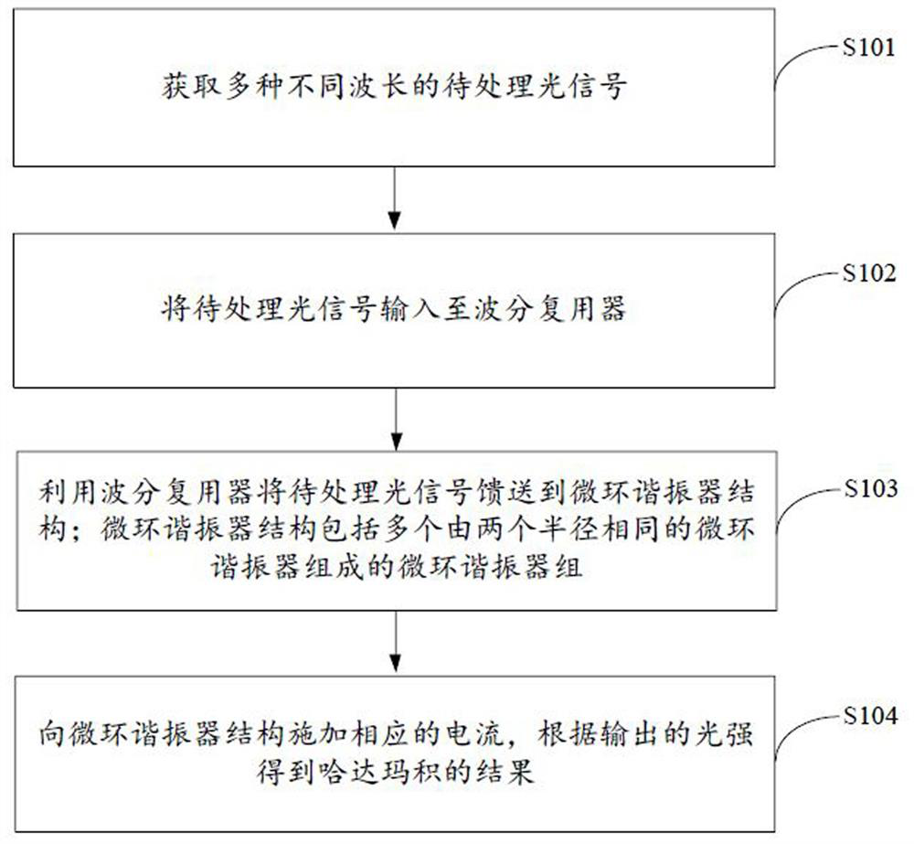
[0033] The present invention provides a realization method of Hadamard product, such as figure 1 shown, including the following steps:

[0034] S101. Obtain multiple optical signals with different wavelengths to be processed;

[0035] S102. Input the optical signal to be processed to a wavelength division multiplexer (Wavelength Division Multiplexing, WDM);

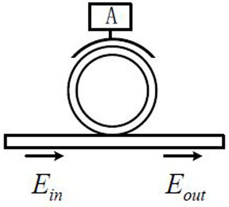
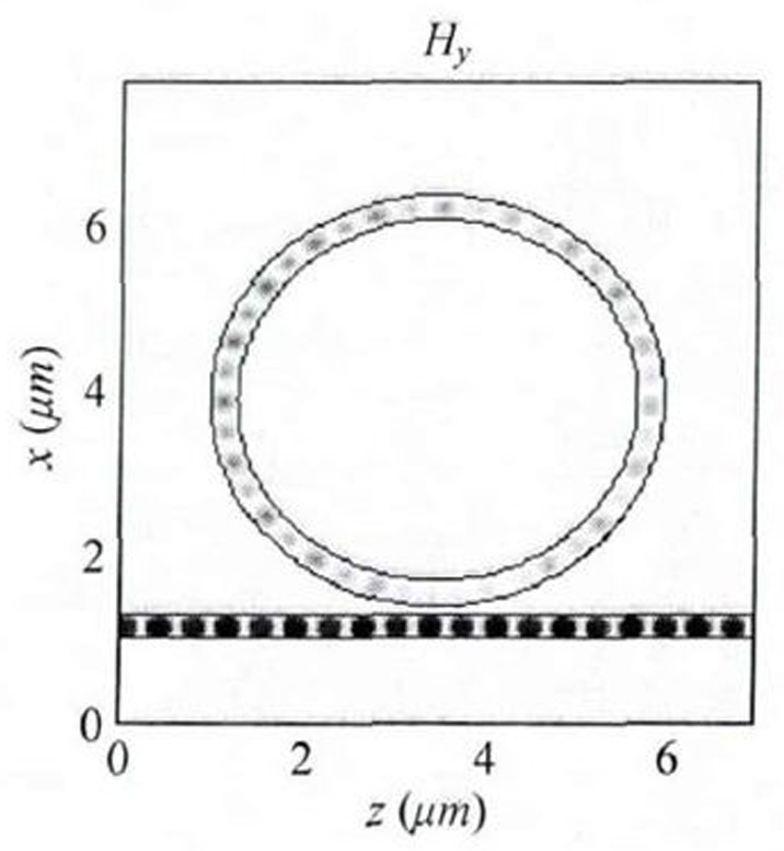
[0036] S103. Using a wavelength division multiplexer to feed the optical signal to be processed to t...


PUM


Abstract

The invention discloses a Hadamard product implementation method and device, and a storage medium. The method comprises the steps of obtaining to-be-processed optical signals of various different wavelengths; inputting a to-be-processed optical signal to a wavelength division multiplexer; feeding a to-be-processed optical signal to the micro-ring resonator structure by using a wavelength division multiplexer, wherein the micro-ring resonator structure comprises a plurality of micro-ring resonator groups consisting of two micro-ring resonators with the same radius; applying corresponding current to the micro-ring resonator structure, and obtaining a Hadamard product result according to the output light intensity. Therefore, the micro-ring resonator is used as the basis for realizing the artificial neural network scheme, the wavelength division multiplexer is used for feeding the optical signal to be processed to the micro-ring resonator structure, the effective refractive index and the phase of the micro-ring resonator can be changed through current heating, and the result of the Hadamard product can be obtained according to the light intensity of the output optical signal; therefore, a simulation solution suitable for the Hadamard product in the optical neural network is realized.

Description

technical field [0001] The invention relates to the technical field of optoelectronic chips, in particular to a Hadamard Product realization method, equipment and storage medium. Background technique [0002] Chips are the foundation and core of the modern electronic information industry. With the rapid development of globalization and technology, the amount of data to be processed is increasing rapidly, and the corresponding data processing models and algorithms are also increasing. As a result, the requirements for computing power and power consumption continue to increase. Photonic computing chips use photons as the information carrier, which has the advantages of high-speed parallelism and low power consumption, so it is considered to be the most promising solution for high-speed, large data volume, and artificial intelligence computing processing in the future. [0003] Today's most common industrial solution for Optical Neural Network (ONN) is to set up proprietary de...

Claims


Application Information

Patent Timeline
Patent Type & Authority Applications(China)
IPC IPC(8): G06N3/067G06F17/16
CPCG06N3/067G06F17/16
Inventor 陈静静吴睿振黄萍王凛
Owner INSPUR SUZHOU INTELLIGENT TECH CO LTD
Why Eureka
Try Eureka