
An ultra-broadband absorber with symmetrical g-bend structure

A technology of ultra-broadband and absorber, applied in the direction of antennas, electrical components, etc., can solve the problem of narrow absorption bandwidth and achieve the effect of wide absorption frequency band, symmetrical structure, and ultra-thin thickness

Active Publication Date: 2022-06-03
BEIJING INSTITUTE OF TECHNOLOGYGY
View PDF12 Cites 0 Cited by
  • Summary
  • Abstract
  • Description
  • Claims
  • Application Information

AI Technical Summary

Problems solved by technology

Although the absorption capacity of the electromagnetic absorber is extremely strong, the resonant absorber mainly relies on the electromagnetic resonance of the metal structure, which has the problem of narrow absorption bandwidth.

Method used


Image

  • An ultra-broadband absorber with symmetrical g-bend structure
  • An ultra-broadband absorber with symmetrical g-bend structure
  • An ultra-broadband absorber with symmetrical g-bend structure

Examples


Embodiment Construction

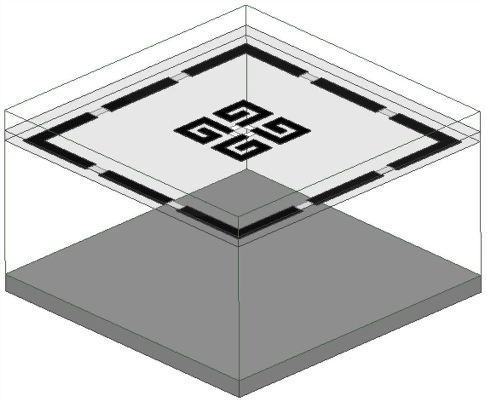
[0022] first combine figure 1 An ultra-broadband wave absorber with a symmetrical G-bend structure according to an embodiment of the present invention will be described. like figure 1 As shown, the ultra-broadband wave absorber includes:

[0023] Upper metal unit, dielectric substrate, lower metal unit, air layer and metal reflector;

[0024] The upper metal unit is attached to the upper surface of the dielectric substrate, and the lower metal unit is attached to the lower surface of the dielectric substrate;

[0025] the air layer is located between the dielectric substrate and the metal reflector;

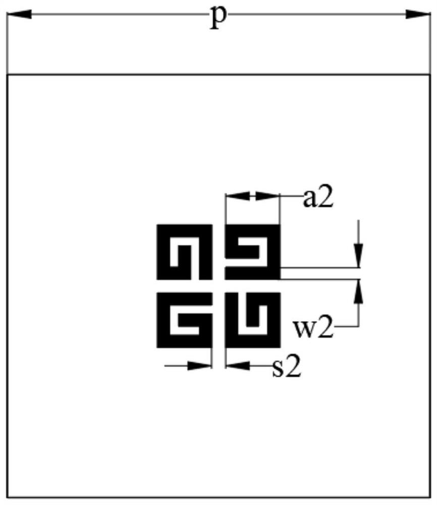
[0026] The upper-layer metal unit is connected to four G-shaped bent metal wires through four chip resistors with equal resistance values, and the G-shaped bent metal wires pass four times in the same direction 90° in the plane where the metal wires are located. bend;

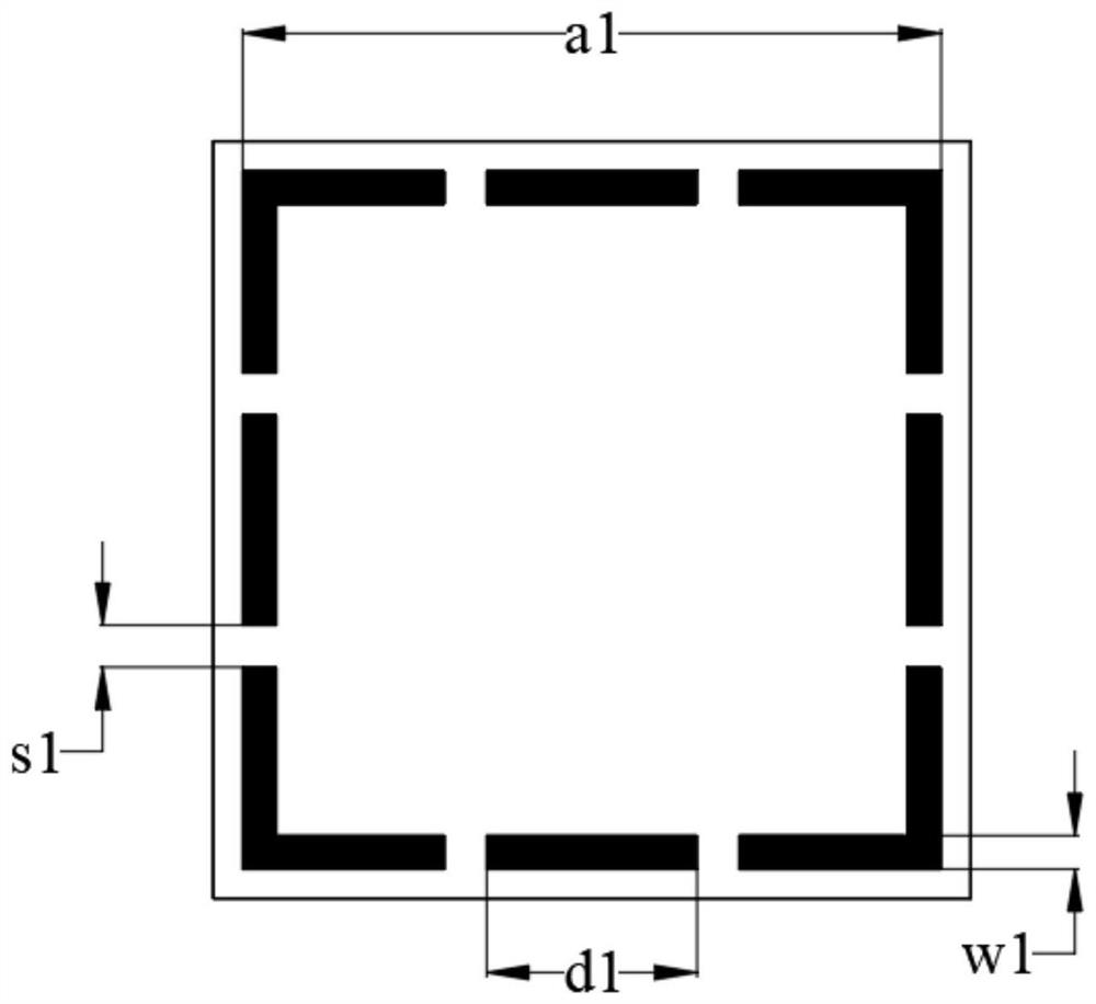
[0027] The lower-layer metal unit is connected to a metal square ring through eight chip resistors with eq...


PUM

PropertyMeasurementUnit
thicknessaaaaaaaaaa
thicknessaaaaaaaaaa

Abstract

The invention provides an ultra-broadband absorber with a symmetrical G-shaped bending structure. The ultra-broadband absorber includes: an upper metal unit, a dielectric substrate, a lower metal unit, an air layer, and a metal reflector; the upper metal The unit is connected to four G-shaped bent metal wires through four chip resistors with equal resistance, and the G-shaped bent metal wires are obtained by bending the metal wires at 90° in the same direction four times in the plane where the metal wires are located; The lower metal unit is connected to a metal square ring through eight chip resistors with equal resistance. According to the solution of the present invention, the ultra-broadband absorber has a symmetrical structure, ultra-thin thickness, insensitive polarization, and wide absorption frequency range.

Description

technical field [0001] The invention relates to the technical field of ultra-broadband electromagnetic wave absorbing, in particular to an ultra-broadband wave absorbing body with a symmetrical G-shaped bending structure. Background technique [0002] Electronic countermeasures have become an important means of combat in modern electronic warfare. Among them, electromagnetic stealth technology is very important. Electromagnetic stealth technology is generally divided into two types: shape stealth and absorbing material stealth. The invisible shape cannot absorb electromagnetic waves, and the electromagnetic waves scattered by the target will still be captured by the multi-station radar. Therefore, absorbing materials that can perfectly absorb incident electromagnetic waves have become a hot research direction. [0003] The rapid development of radar technology has put forward higher and higher requirements for absorbing materials. Traditional absorbing materials have expose...

Claims


Application Information

Patent Timeline
Patent Type & Authority Patents(China)
IPC IPC(8): H01Q17/00H01Q15/00
CPCH01Q17/00H01Q15/0086H01Q15/0026
Inventor 任武王沛沛李伟明薛正辉郝艺茗相明旭
Owner BEIJING INSTITUTE OF TECHNOLOGYGY
Learn More