
Data read-write control circuit for flash type programmable logic device

A technology for data reading, writing and control circuits, applied in instruments, static memory, read-only memory, etc., can solve problems such as single function, and achieve the effect of flexibility

Pending Publication Date: 2021-09-24
WUXI ESIONTECH CO LTD +1
View PDF0 Cites 0 Cited by
  • Summary
  • Abstract
  • Description
  • Claims
  • Application Information

AI Technical Summary

Problems solved by technology

In the clearing phase, the output of all storage units FlashCell is 0. In the data configuration phase, the read-write control circuit configuration bit stream is loaded to the data shift register DSR, and then configured to the storage unit FlashCell through the address decoder ASR. The read-write control circuit mainly implements the basic configuration of the storage function, and the function is relatively single. However, many existing complex integrated circuit chips need to load configuration information after the chip is reset, or reload the specified configuration information in the working state. The current configuration It is difficult for the read and write control circuit in the memory to meet this functional requirement

Method used


Image

  • Data read-write control circuit for flash type programmable logic device
  • Data read-write control circuit for flash type programmable logic device
  • Data read-write control circuit for flash type programmable logic device

Examples


Embodiment Construction

[0015] The specific embodiments of the present invention will be further described below in conjunction with the accompanying drawings.

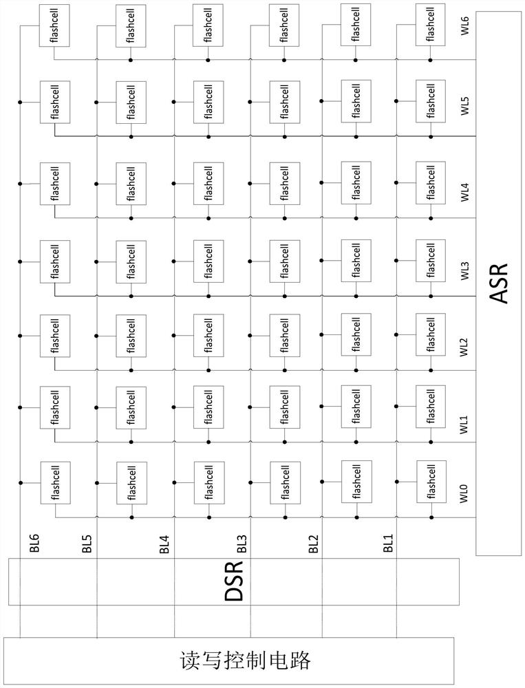
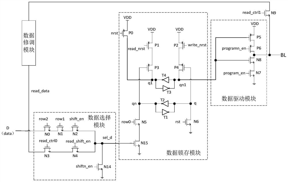
[0016] This application discloses a data read and write control circuit for flash programmable logic devices, please refer to figure 2 , the data reading and writing control circuit includes a data selection module, a data latch module, a data drive module, a readback control module and a data trimming module. Wherein, the data selection module includes a configuration data channel and a write-back data channel, and the input terminal of the configuration data channel is used as the data terminal D of the data read-write control circuit to obtain configuration data data. The output end of the configuration data channel is connected to the output end of the write-back data channel and connected to the input end of the data latch module, and the data sel_d obtained by the input end of the data latch module is the selected data. The output te...


PUM


Abstract

The invention discloses a data read-write control circuit for a flash type programmable logic device, and relates to the field of programmable logic devices.The data read-write control circuit is characterized in that when the data read-write control circuit performs data write-in, a data selection module gates a configuration data channel to write configuration data into a data latch module for latching; and outputting corresponding configuration data through a data driving module; when the data read-write control circuit carries out data write-back, transmitting the configuration data at the output end of the output control module to a data trimming module through a read-back control module for data trimming, and obtaining trimmed configuration data; gating the write-back data channel by the data selection module to write the trimmed configuration data into the data latching module for latching, and then outputting the trimmed configuration data through the data driving module, and the data read-write control circuit can realize stable data configuration and data write-back, does not occupy an additional register unit, is flexible to realize, and is suitable for large-scale programmable devices.

Description

technical field [0001] The invention relates to the field of programmable logic devices, in particular to a data read-write control circuit for flash programmable logic devices. Background technique [0002] Programmable logic devices are designed based on repeated configuration storage technology, and can complete circuit modification by re-downloading programming. It has the advantages of short development cycle, low cost, low risk, and easy maintenance and upgrade of electronic systems, so it has become the mainstream of integrated circuit chips. . [0003] The configuration memory architecture of existing programmable logic devices such as figure 1 As shown, it mainly includes the storage array composed of read-write control circuit, data shift register DSR, address decoder ASR, and storage unit FlashCell. Because it is widely distributed and spreads all over the chip, the specific number of cascaded stages is related to the size of the chip capacity. . In the clearin...

Claims


Application Information

Patent Timeline
IPC IPC(8): G11C7/10G11C16/10
CPCG11C7/1006G11C7/1087G11C16/10
Inventor 何小飞曹正州
Owner WUXI ESIONTECH CO LTD
Features
  • Generate Ideas
  • Intellectual Property
  • Life Sciences
  • Materials
  • Tech Scout
  • Unparalleled Data Quality
  • Higher Quality Content
  • 60% Fewer Hallucinations
Learn More