Polymer, semiconductor composition comprising polymer, and method for manufacturing film using semiconductor composition

A polymer and bonding technology, applied in the field of polymers, can solve the problem of not recording the required characteristics of the underlying anti-reflection film, and achieve the effects of improving flatness, reducing sublimation, and reducing standing waves

Pending Publication Date: 2021-09-28
MERCK PATENT GMBH
View PDF13 Cites 0 Cited by
  • Summary
  • Abstract
  • Description
  • Claims
  • Application Information

AI Technical Summary

Problems solved by technology

Although Patent Document 2 discloses a composition for forming a fine resist pattern having a specific polymer, it does not describe whether it can form a lower antireflection film or whether it has the required properties as a lower antireflection film.

Method used


Image

  • Polymer, semiconductor composition comprising polymer, and method for manufacturing film using semiconductor composition
  • Polymer, semiconductor composition comprising polymer, and method for manufacturing film using semiconductor composition
  • Polymer, semiconductor composition comprising polymer, and method for manufacturing film using semiconductor composition

Examples


Embodiment

[0269] The present invention will be described below by way of various examples. Aspects of the invention are not limited to these examples.

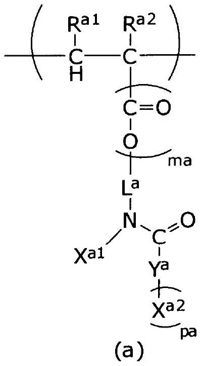
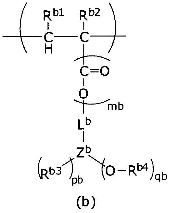
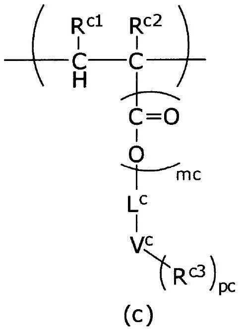
[0270] Synthesis of Polymer 1

[0271] Add 350g PGMEA in the three-necked flask, then add the following MOI-BP (Karenzu MOI-BP, Showa Denko) 32.79g, McHN (Kawasaki Chemical Industry) 20g, DYE-M9A (Osaka Shinyaku) 6.422g, HPMA (Light Ester HOP, Kyoeisha Chemical) 8.16g. They correspond to unit (a), unit (b), unit (c) and unit (d), respectively.

[0272]

[0273] Furthermore, V-601 / oil-soluble azo polymerization initiator (Fujifilm Wako Pure Chemical Industries, Ltd.) was added. Charge nitrogen into the three-necked flask, cover the lid, heat while stirring, and react at 80° C. for 4 hours. Additionally, 3 g of PGME was added and stirred to complete the polymerization. The reaction solution was brought back to room temperature. The reaction solution was added dropwise to 1500 g of hexane to precipitate a polymer. It was filtered...


PUM

PropertyMeasurementUnit
thicknessaaaaaaaaaa
thicknessaaaaaaaaaa
thicknessaaaaaaaaaa

Abstract

The present invention provides a novel polymer capable of reducing sublimate during film formation and a composition comprising the same. The polymer (A) according to the present invention comprises at least one structural unit selected from the group consisting of Unit (a), Unit (b), Unit (c) and Unit (d) having certain structures, wherein, n a, n b, n c and n d, which are the numbers of repetition respectively of Units (a), (b), (c) and (d), satisfy the following formulae: na+nb>0, n c>=0 and n d>=0.

Description

technical field [0001] The present invention relates to a polymer containing a specific structural unit, and a semiconductor composition containing the polymer. In addition, the present invention relates to a film using the semiconductor composition and a method for manufacturing a device. Background technique [0002] In the manufacturing process of devices such as semiconductors, fine processing is usually performed by photolithography using photoresists. The process of microfabrication is to form a thin photoresist layer on a semiconductor substrate such as a silicon wafer, cover this layer with a mask pattern corresponding to the pattern of the device targeted at this layer, and activate it with ultraviolet light or the like through the mask pattern. This layer is exposed to light, a photoresist pattern is obtained by developing the exposed layer, and the substrate is etched using the obtained photoresist pattern as a protective film, thereby forming fine unevenness cor...

Claims


Application Information

Patent Timeline
Patent Type & Authority Applications(China)
IPC IPC(8): C08F220/26C08F220/30C08F220/34G03F7/09
CPCG03F7/091C08F220/26C08F220/54C08F220/346C08F220/365G03F7/0382G03F7/0392H01L21/0274C08F220/281C08F220/301G03F7/0045G03F7/2006G03F7/32H01L21/0276H01L21/3081H01L21/3086
Inventor 仁川裕片山朋英矢野友嗣张锐菱田有高铃木理人小崎力生冈村聪也
Owner MERCK PATENT GMBH
Why Eureka
Try Eureka