A partial discharge suppression method at the flange of a gis/gil support insulator
A technology supporting insulators and partial discharges, applied in insulators, processing data acquisition/processing, circuits, etc., can solve problems such as difficulty in hindering the movement of micron-level particles, and achieve high-precision manufacturing, high interface bonding strength, and compatibility Good results
- Summary
- Abstract
- Description
- Claims
- Application Information
AI Technical Summary
Problems solved by technology
Method used
Image
Examples
Embodiment 1
[0076] Example 1: 110kV Disc Support Insulator
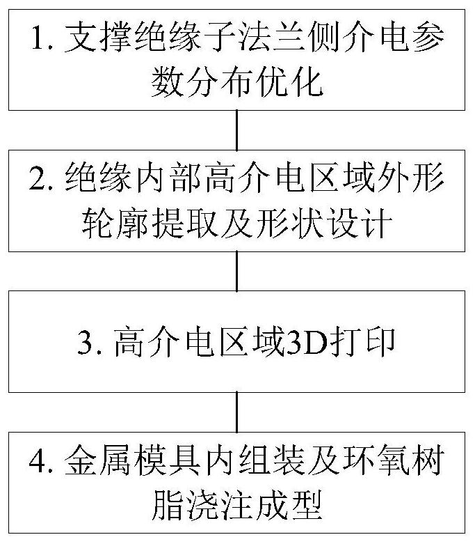
[0077] 1) Optimization of the dielectric parameter distribution on the flange side of the supporting insulator
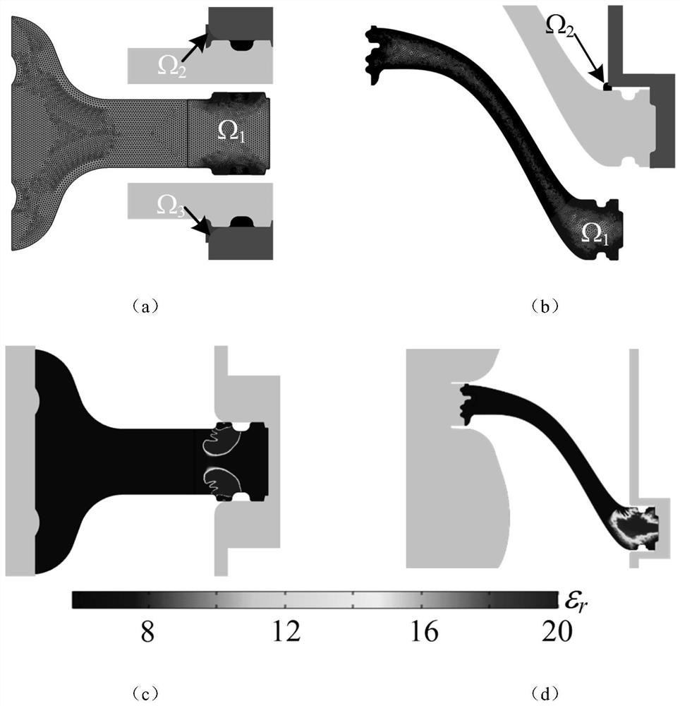
[0078] The two-dimensional axisymmetric structure of the 110kV disc-supported insulator is as follows: figure 2 As shown in (a), taking the optimized dielectric constant as an example, the root Ω of the supporting insulator 1 The area is the design feasible area, and the area indicated by the arrow is the optimization target area Ω 2 and Ω 3 , the mathematical description of the optimization problem is as in Equation 1, and the design variable is the design feasible region Ω 1 The permittivity in any grid in the inner, optimization objective is divided into two parts, f 1 is the electric field integral term, which is used to reduce the optimization target area Ω 2 and Ω 3 The value of the electric field in the . C ref1 and C ref2 respectively f 1 The normalization parameters of the two optimization componen...
Embodiment 2
[0089] Example 2: 110kV Basin Support Insulator
[0090] 1) Optimization of the dielectric parameter distribution on the flange side of the supporting insulator
[0091] The 110kV disk-type supporting insulator is taken as an example to optimize the dielectric constant. 1 The area is the design feasible area, and the area indicated by the arrow is the optimization target area Ω 2 and Ω 3 , the mathematical description of the optimization problem is shown in Equation 3, and the design variable is the design feasible region Ω 1 The permittivity in any grid in the inner, optimization objective is divided into two parts, f 1 is the electric field integral term, which is used to reduce the optimization target area Ω 2 and Ω 3 The value of the electric field in the . C ref1 and C ref2 respectively f 1 The normalization parameters of the two optimization components in the middle are so that the value obtained in the initial calculation process is 1, thereby improving the con...
Embodiment 3
[0102] Example 3: 550kV Basin Support Insulator
[0103] 1) Optimization of the dielectric parameter distribution on the flange side of the supporting insulator
[0104] The two-dimensional axisymmetric structure of the 550kV basin support insulator is as follows: figure 2 As shown in (b), taking the optimized dielectric constant as an example, the root Ω of the supporting insulator 1 The area is the design feasible area, and the area indicated by the arrow is the optimization target area Ω 2 , the mathematical description of the optimization problem is shown in Equation 5, and the design variable is the design feasible region Ω 1 The permittivity in any grid in the inner, optimization objective is divided into two parts, f 1 is the electric field integral term, which is used to reduce the optimization target area Ω 2 and Ω 3 The value of the electric field in the . C ref for f 1 The normalization parameters of the two optimization components in the middle are so that...
PUM
 Abstract
Description
Claims
Application Information


