Radio frequency switch circuit for optimizing voltage withstanding uniformity of stacked switch tubes

A radio frequency switch and uniformity technology, applied in electronic switches, electrical components, pulse technology, etc., can solve problems such as damage to transistor devices, uneven maximum peak voltage, and reduce the maximum input power of radio frequency switches, so as to improve the uniformity of withstand voltage Effect

Pending Publication Date: 2021-10-01
上海迦美信芯通讯技术有限公司
View PDF0 Cites 4 Cited by
  • Summary
  • Abstract
  • Description
  • Claims
  • Application Information

AI Technical Summary

Problems solved by technology

Taking the simplest single-pole single-throw SPST RF switch as an example, its disadvantage is that when the RF switch is in the off state VG1=VG2=-2.5V, when a high-power RF signal enters from the RF1 or RF2 end, the series branch module The maximum peak voltage borne by each stage of switching transistors stacked with the parallel branch module is not uniform, especially the maximum peak voltage borne by the switching transistors of the first and last stages of stacked transistors is much greater than the average value, which will reduce the radio frequency The maximum input power that the switch can handle may even damage the transistor devices inside the RF switch

Method used


Image

  • Radio frequency switch circuit for optimizing voltage withstanding uniformity of stacked switch tubes
  • Radio frequency switch circuit for optimizing voltage withstanding uniformity of stacked switch tubes
  • Radio frequency switch circuit for optimizing voltage withstanding uniformity of stacked switch tubes

Examples


Embodiment Construction

[0023] The following will clearly and completely describe the technical solutions in the embodiments of the present invention with reference to the accompanying drawings in the embodiments of the present invention. Obviously, the described embodiments are only some, not all, embodiments of the present invention. Based on the embodiments of the present invention, all other embodiments obtained by persons of ordinary skill in the art without creative efforts fall within the protection scope of the present invention.

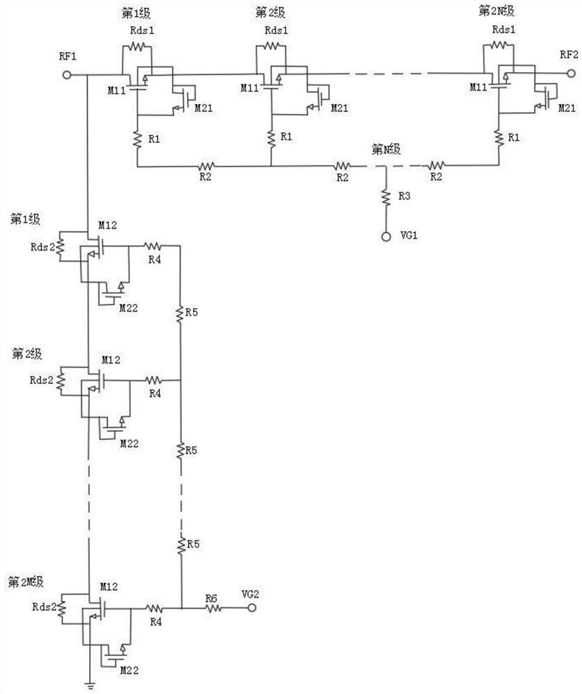
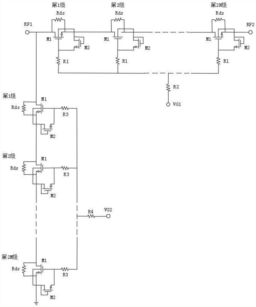
[0024] Such as figure 2 As shown, it is a traditional single-pole single-throw SPST RF switch. Its disadvantage is that the RF switch is in the off state VG1=VG2=-2.5V. When a high-power RF signal enters from the RF1 or RF2 end, the series branch module The maximum peak voltage borne by each stage of switching transistors stacked with the parallel branch module is not uniform, especially the maximum peak voltage borne by the switching transistors of the first and ...


PUM


Abstract

The invention discloses a radio frequency switch circuit for optimizing voltage withstanding uniformity of stacked switch tubes, and relates to the technical field of radio frequency integrated circuits. The circuit comprises a series branch module composed of 2N first switch transistors, a first bias transistor, a first source drain resistor, a first grid bias resistor, 2N-1 first grid series resistors and a first grid common end resistor; a parallel branch module composed of 2M second switch transistors, a second bias transistor, a second source drain resistor, a second grid bias resistor, 2M-1 second grid series resistors and a second grid common end resistor; according to the structure, the maximum peak voltage borne by the switch transistors of the previous stages and the later stages of the radio frequency switch can be reduced, the withstand voltage uniformity of each stage of switch transistor of the radio frequency switch and the maximum input power of the radio frequency switch are improved, and particularly, the withstand voltage uniformity of each stage of switch transistor of a parallel branch module is improved.

Description

technical field [0001] The invention belongs to the technical field of radio frequency integrated circuits, and in particular relates to a radio frequency switch circuit for optimizing the pressure uniformity of stacked switch tubes. Background technique [0002] With the continuous development of wireless mobile communication technology, RF switches play an increasingly important role in multi-band front-end modules and antenna tuners. Especially in the multi-scenario application of antenna tuners, high power handling capability has become an important research direction of RF switches. [0003] Stacking transistors is a commonly used method to improve the power handling capability of RF switches. Taking the simplest single-pole single-throw SPST RF switch as an example, its disadvantage is that when the RF switch is in the off state VG1=VG2=-2.5V, when a high-power RF signal enters from the RF1 or RF2 end, the series branch module The maximum peak voltage borne by each s...

Claims


Application Information

Patent Timeline
Patent Type & Authority Applications(China)
IPC IPC(8): H03K17/10H03K17/687
CPCH03K17/102H03K17/687
Inventor 沈宇管剑铃谢婷婷王玉娇周德杭倪成东倪文海徐文华
Owner 上海迦美信芯通讯技术有限公司
Why Eureka
Try Eureka