Method for improving flatness of back surface of wafer

A flatness, wafer technology, applied in the direction of electrical components, semiconductor/solid-state device manufacturing, circuits, etc., can solve the problems of uneven flatness on the back of the wafer, out-of-focus graphics, poor etching effect, etc., to eliminate Defocus Effects of defects, flatness improvement, and uniform thickness

Pending Publication Date: 2021-10-15
SHANGHAI HUALI INTEGRATED CIRCUTE MFG CO LTD
View PDF3 Cites 4 Cited by
  • Summary
  • Abstract
  • Description
  • Claims
  • Application Information

AI Technical Summary

Problems solved by technology

In the process of washing off the SMT silicon nitride film layer by the acid bath process, since the front and back of the wafer are soaked in the cleaning solution at the same time, the cleaning solution will also clean the silicon nitride film layer on the back of the wafer. The polysilicon gate film (Poly) is exposed, but due to the limited cleaning process, the silicon nitride film layer on the back of the wafer cannot be completely removed, and there will be residues of the silicon nitride film layer, especially at the edge of the wafer, where the residue is more obvious , and the residual silicon nitride film layer will remain until the back-end process; in the factory where the front-end and back-end processes share the lithography machine, the back of the wafer must be cleaned before the back-end wafer enters the lithography machine In order to reduce the concentration of metal ions to a safe range, and during the cleaning process, the cleaning solution will also etch the Poly. When there is a silicon nitride film layer on the Poly, the etching effect of the cleaning solution on the Poly will become worse. Therefore, the etched thickness of Poly without silicon nitride thin film layer and Poly with silicon nitride thin film layer will be different after being etched, resulting in uneven overall flatness on the back of the wafer, especially the residual silicon nitride thin film layer. serious borderline
After entering the photolithography process, the abnormal flatness of the back of the wafer is likely to cause pattern out-of-focus (Defocus) defects, which in turn affects the overall yield of the wafer. Although it can be remedied by photolithography rework, the amount of remediation is only a small part. And the cost is extremely high, still can't fundamentally solve the problem
In order to reduce the impact caused by abnormal flatness on the back of the wafer, in the cleaning step before the wafer enters the lithography machine, an attempt was made to control the etching amount of the cleaning solution on Poly by diluting the concentration of the cleaning solution to improve the flatness. The effect is not ideal, and after the cleaning solution is diluted, the removal effect on metal ions becomes worse, and even the concentration of metal ions cannot be controlled within the standard range. Therefore, it is necessary to further explore how to improve the flatness of the back of the wafer

Method used


Image

  • Method for improving flatness of back surface of wafer
  • Method for improving flatness of back surface of wafer
  • Method for improving flatness of back surface of wafer

Examples


Embodiment Construction

[0031] The technical solutions in the present invention will be clearly and completely described below in conjunction with the accompanying drawings. Apparently, the described embodiments are part of the embodiments of the present invention, not all of them. Based on the embodiments of the present invention, all other embodiments obtained by persons of ordinary skill in the art without making creative efforts belong to the protection scope of the present invention.

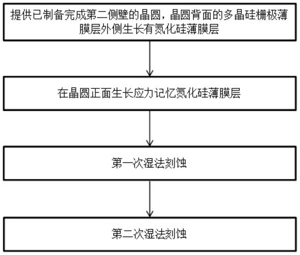
[0032] refer to figure 2 , showing the method for improving the flatness of the wafer backside of the present invention, comprising the steps of:

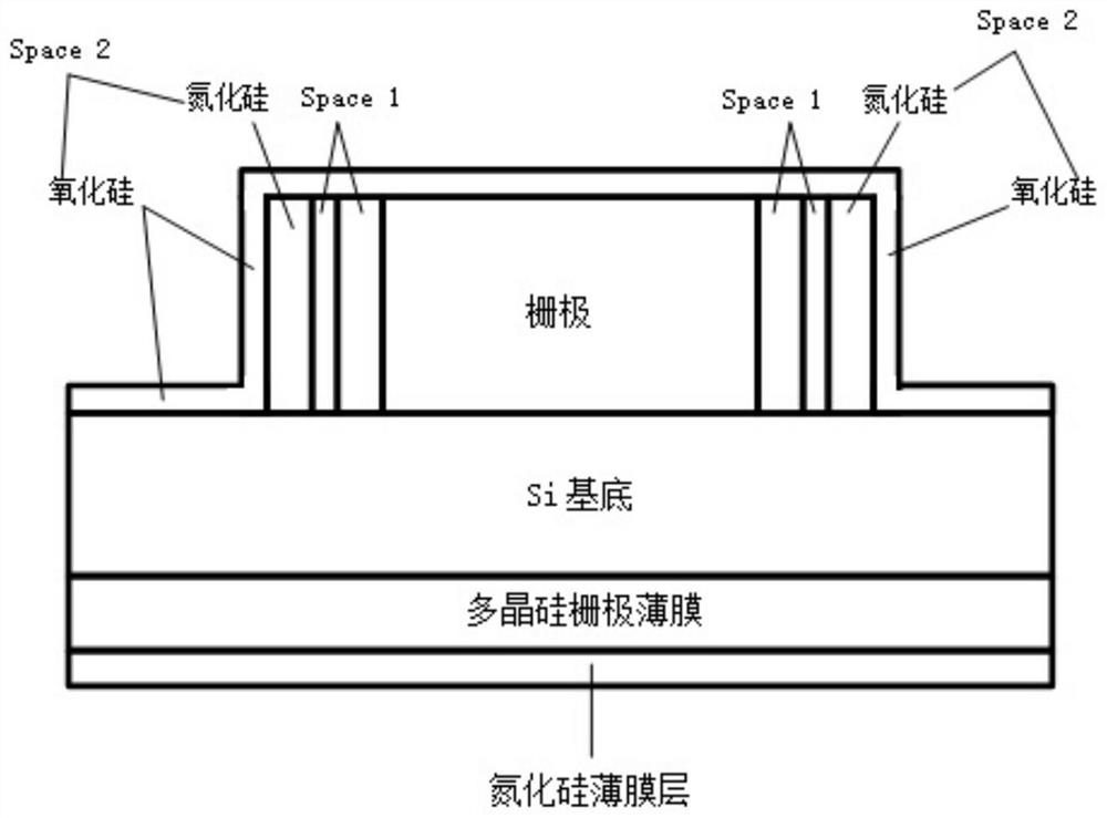
[0033] Step A, providing a wafer with the second side wall prepared, and a silicon nitride film layer is grown on the outside of the polysilicon gate film layer on the back of the wafer;

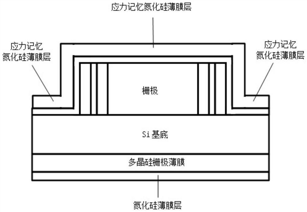
[0034] Step B, growing a stress-memory silicon nitride film layer on the front side of the wafer provided in step A, the cross-sectional structure schematic diagram of the wafer is...


PUM


Abstract

The invention discloses a method for improving the flatness of the back surface of a wafer. The method comprises the following steps of: growing a stress memory silicon nitride thin film layer on the front surface of the wafer on which a second side wall is grown; removing the stress memory silicon nitride thin film layer and the silicon nitride thin film layer through first-time etching; and removing the residual silicon nitride film layer on the back surface of the wafer through second wet etching. According to the method, a cleaning process for the back surface of the wafer is added after an acid tank cleaning process, so that the silicon nitride thin film layer on the back surface of the wafer which is not completely removed in the acid tank process can be completely removed, and after the silicon nitride thin film layer is removed, the wafer is cleaned before entering a photoetching machine in a rear-section process; and therefore, the etching effect of the cleaning liquid on the Poly is not influenced by the residual silicon nitride thin film layer, so that the thickness of the Poly is uniform, the flatness of the back surface of the wafer is improved, the Defocus defect is reduced or eliminated, and the yield is improved.

Description

technical field [0001] The invention relates to the field of wafer manufacturing, in particular to a method for improving the flatness of the wafer back. Background technique [0002] The second sidewall (Space 2) of the wafer generally includes a silicon nitride film layer and a silicon oxide film layer, which are mainly formed by deposition and etching processes on the surface of the wafer on which the first sidewall (Space 1) is formed, figure 1 A schematic cross-sectional structure of a wafer with Space 2 is shown. Among them, the silicon nitride thin film layer is generally prepared by a furnace tube process, therefore, the silicon nitride thin film layer is deposited on both the front and back sides of the wafer. [0003] At the same time, in order to increase the speed of semiconductor devices, a stress memory (SMT) silicon nitride film layer is deposited on the front of the wafer. The SMT silicon nitride film layer has tensile stress, and then through a rapid anneal...

Claims


Application Information

Patent Timeline
Patent Type & Authority Applications(China)
IPC IPC(8): H01L21/02
CPCH01L21/0206H01L21/0209H01L21/02318
Inventor 陆尉徐晓林周维
Owner SHANGHAI HUALI INTEGRATED CIRCUTE MFG CO LTD
Why Eureka
Try Eureka