

A method and device for processing LED chips on sapphire substrates
A technology for LED chips and sapphire substrates, applied in the field of processing sapphire substrate LED chips, can solve the problems of chip leakage, micro-crack expansion, affecting luminous efficiency, etc., to meet high-precision processing requirements, stable and reliable driving, and motion accuracy. high effect
- Summary
- Abstract
- Description
- Claims
- Application Information
AI Technical Summary
Problems solved by technology
Method used
Image

Examples
Embodiment 1
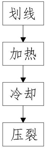
[0050] refer to figure 1 , a method for processing a sapphire substrate LED chip is proposed in this embodiment, comprising the following steps:
[0051] S1: First, use a scribing laser to scribe on the sapphire surface of the LED wafer, and form deep initial cracks on the sapphire surface of the LED wafer;
[0052] S2: heating the initial crack and the sapphire surface of the LED wafer on both sides along the extension direction of the initial crack;
[0053] S3: cooling the initial crack and the sapphire surface of the LED wafer on both sides along the extension direction of the initial crack;
[0054] S4: Use the diamond cutter 500 to separate the LED wafer, and distribute the diamond cutter 500 and the surface of the LED wafer vertically. The diamond tool 500 is struck until the LED wafer is separated, so that the LED wafer is cracked along the corresponding initial cracks.
[0055] In S1, a scribing laser with a wavelength of 200-1000nm is used for scribing, and the de...
Embodiment 2
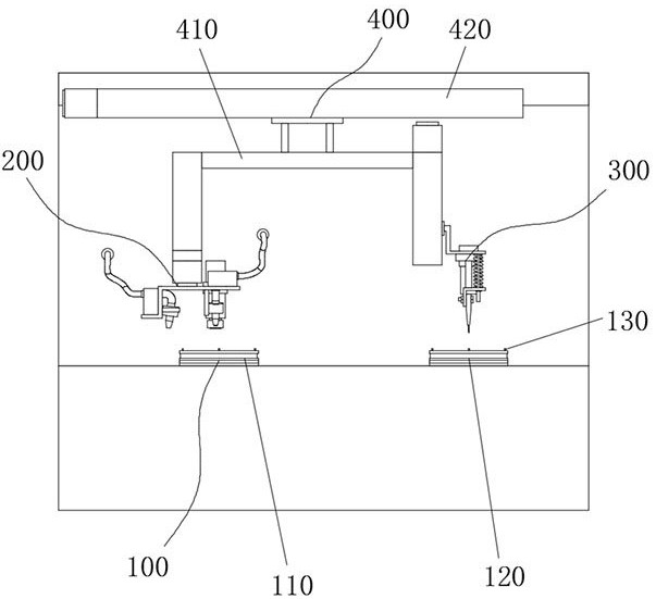
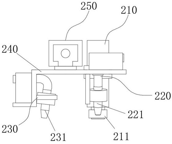
[0058] refer to figure 2 In this embodiment, a device for processing LED chips on a sapphire substrate is proposed, which includes two processing turntables 100 arranged side by side. The A-turntable 110 and the B-turntable 120 are arranged at intervals along the a direction, and the a-direction is located in the horizontal plane. The A-turntable 110 and the B-turntable 120 are equipped with a clamping mechanism 130 for fixing and limiting the LED wafer, above the A-turntable 110 A processing mechanism 200 is installed, and the A processing mechanism 200 is used for scribing, heating and cooling the LED wafer on the A turntable 110, and a B processing mechanism 300 is installed above the B turntable 120, and the B processing mechanism 300 is used for B processing. The LED wafer on the turntable 120 is subjected to fracturing treatment, the A processing mechanism 200 and the B processing mechanism 300 are connected to the adjustment mechanism 400, and the adjustment mechanism ...
PUM
| Property | Measurement | Unit |
|---|---|---|
| wavelength | aaaaa | aaaaa |
| Mohs hardness | aaaaa | aaaaa |
Abstract
Description
Claims
Application Information