

Method of manufacturing semiconductor device
a manufacturing method and semiconductor technology, applied in the direction of semiconductor devices, basic electric elements, electrical appliances, etc., can solve the problems of reducing the contact resistance, etc., to improve the reliability of the semiconductor device, reduce the resistance of the metal silicide layer, and reduce the diffusion resistance
- Summary
- Abstract
- Description
- Claims
- Application Information
AI Technical Summary
Benefits of technology
Problems solved by technology
Method used
Image

Examples
first embodiment
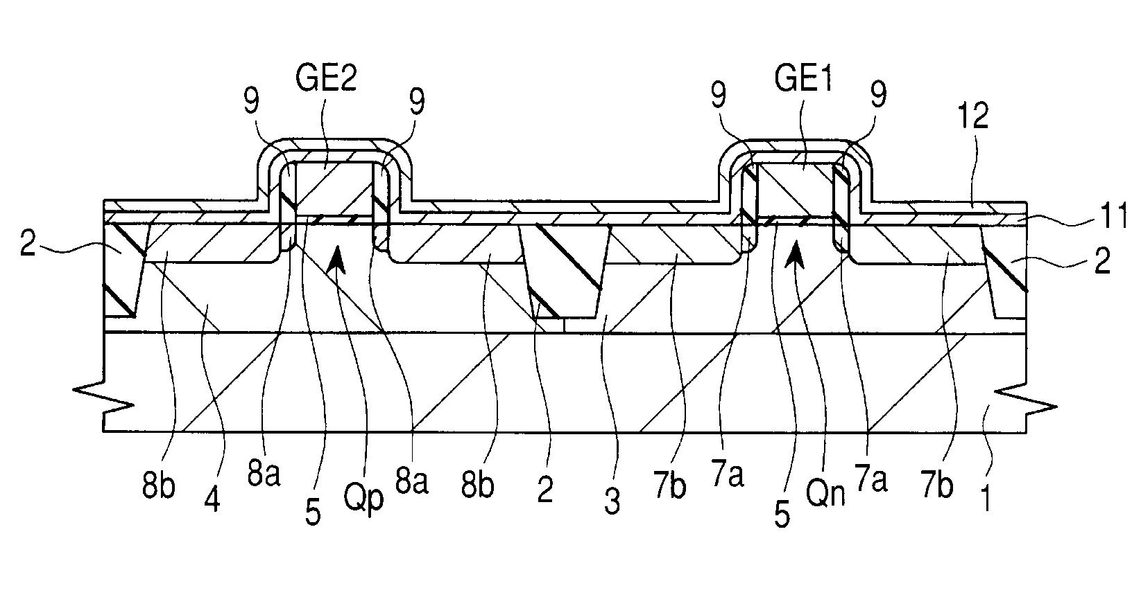
[0082]A manufacturing procedure of a semiconductor device according to this embodiment will be described below with reference to the accompanying drawings. FIGS. 1 to 5 are cross-sectional views showing main parts of the semiconductor device during the manufacturing procedure thereof device according to one embodiment of the invention, for example, the semiconductor device including a complementary metal insulator semiconductor field effect transistor (CMISFET).
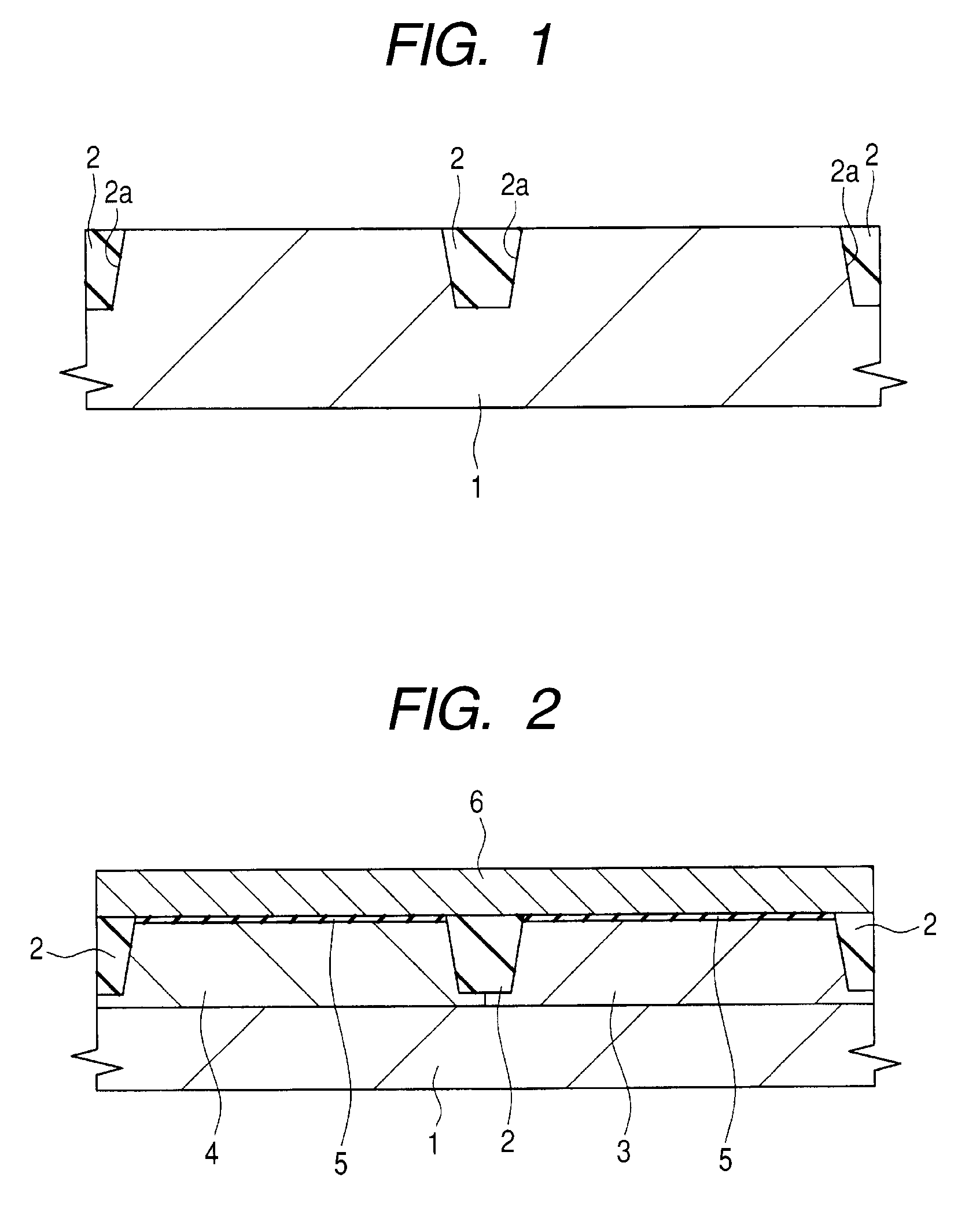
[0083]First, as shown in FIG. 1, a semiconductor substrate (semiconductor wafer) 1 including a p-type single crystal silicon or the like having a specific resistance of, for example, about 1 to 10 Ωcm is prepared. Element isolation regions 2 are formed at a main surface of the semiconductor substrate 1. The element isolation region 2 is formed of an insulator, such as silicon oxide, for example, by a shallow trench isolation (STI) method, or by a local oxidization of silicon method (LOCOS) method. For example, an insulating f...
second embodiment
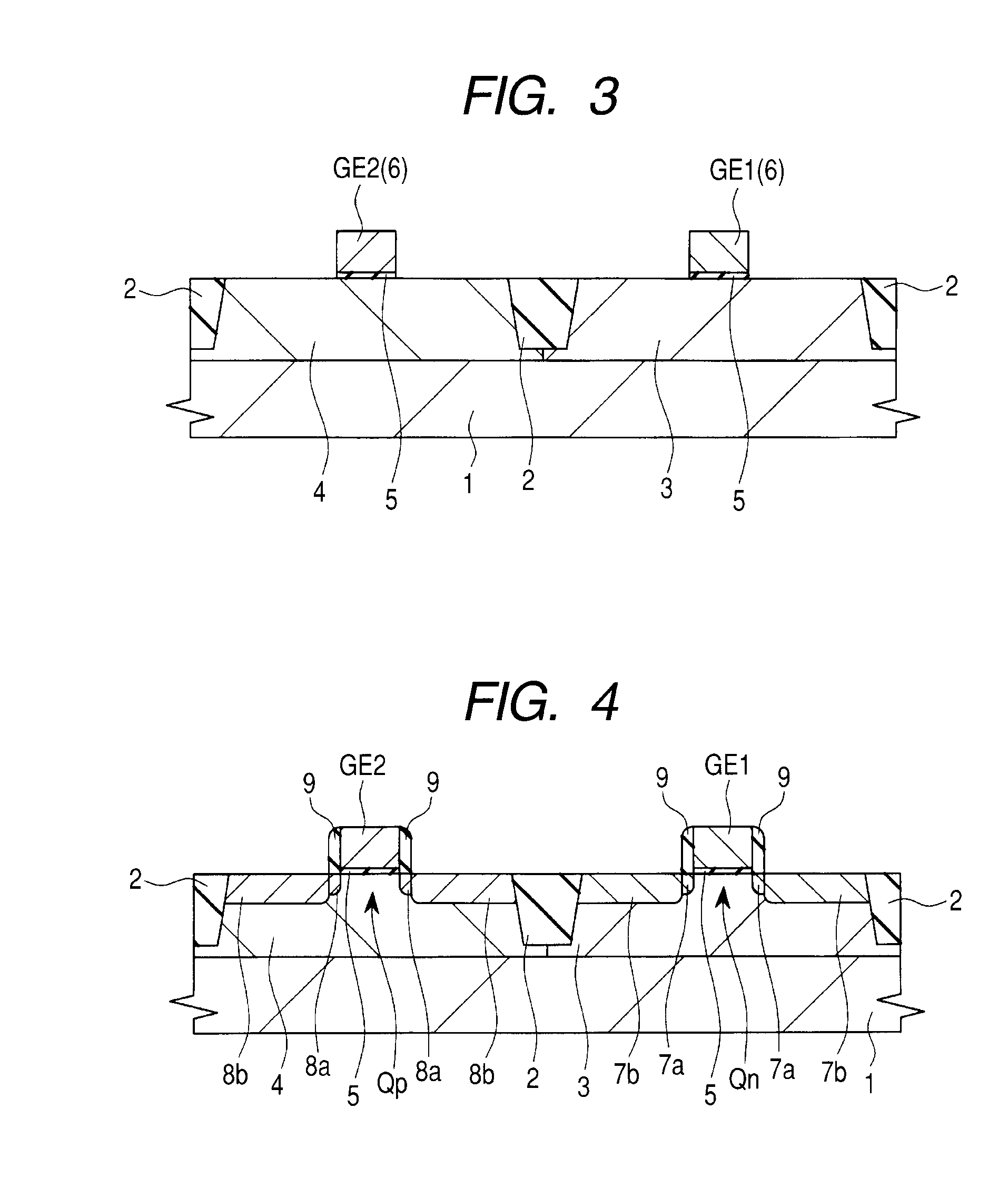
[0245]FIGS. 52 to 56 are cross-sectional diagrams of main parts of a semiconductor device in a manufacturing procedure thereof in this embodiment. FIG. 52 corresponds to the same process step of the procedure as that shown in FIG. 4. FIG. 56 corresponds to the same process step of the procedure as that shown in FIG. 12.
[0246]The same processes as those of the first embodiment described with reference to FIGS. 1 to 4 are performed thereby to obtain the structure of FIG. 52 corresponding to that shown in FIG. 4. The structure of an n-channel MISFETQn shown in FIG. 52 is substantially the same as that described in the first embodiment, and a description thereof will be omitted below. Also, in this embodiment, not only the n-channel MISFETQn, but also the above-mentioned p-channel MISFETQp can be formed like the first embodiment. It is noted that for simplification, the illustration and description of the p-channel MISFETQp will be omitted.
[0247]In this embodiment, the silicon film 6 is...
PUM
 Abstract
Description
Claims
Application Information