Systems and methods for encapsulating electronic component
A technology for electronic components and packaging electronics, which is applied in chemical instruments and methods, electronic equipment, electrical components, etc., and can solve problems such as the undesired thickness of the packaging layer.
- Summary
- Abstract
- Description
- Claims
- Application Information
AI Technical Summary
Problems solved by technology
Method used
Image

Examples
Embodiment 1
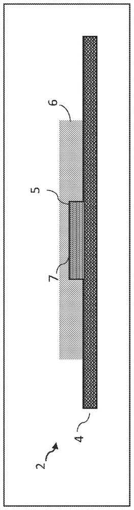
[0093] The encapsulated article of Example 1 was prepared using a HARDO T150 application system (Hardo, Bad Salzburg, Germany) including a main tank, mixing roll, applicator roll and doctor blade to apply encapsulation composition 3 to the substrate 4 on. The mixing roll was set to 140°C. Position the doctor blade so that the distance from the doctor blade to the applicator roll is 0.45 mm. The size of the gap between the application roller and the substrate 4 is 0.2 mm.
[0094] To prepare the encapsulated article of Example 1, Encapsulation Composition 3 was heated to a temperature of 140°C until it was completely melted and in liquid form. The substrate 4 was then transferred to the applicator roller at a linear rate of 3.5 meters per minute (m / min) while being supported from below in such a way that the substrate 4 passed under the applicator roller as horizontally as possible. As the substrate 4 passed under the application rollers, the encapsulation composition 3 was ...
Embodiment 2
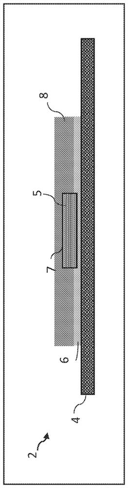
[0096] The encapsulated article of Example 2 was prepared in substantially the same manner as described in Example 1 above, except that after the encapsulation layer was formed on the substrate 4, while the encapsulation layer was still hot, 100 mm long x 40 mm wide x A 0.2 mm thick thin film solar array was placed on the encapsulation layer.
[0097] The size of the gap between the substrate and the application roller was then set to 0.4 mm and the substrate with the thin film solar array positioned on top of the encapsulation layer was passed under the application roller of the HARDO T150 application system and the encapsulation composition was 3 is applied on the thin film solar array to encapsulate the thin film solar array with the layer of encapsulating composition 3 . The resulting construction was passed through the system two additional times, during which time two additional layers of encapsulating composition 3 were applied to the construction. The gap between the ...
PUM
| Property | Measurement | Unit |
|---|---|---|
| melt flow index | aaaaa | aaaaa |
| thickness | aaaaa | aaaaa |
Abstract
Description
Claims
Application Information
 - R&D
- Intellectual Property
- Life Sciences
- Materials
- Tech Scout
- Unparalleled Data Quality
- Higher Quality Content
- 60% Fewer Hallucinations
Browse by: Latest US Patents, China's latest patents, Technical Efficacy Thesaurus, Application Domain, Technology Topic, Popular Technical Reports.
© 2025 PatSnap. All rights reserved.Legal|Privacy policy|Modern Slavery Act Transparency Statement|Sitemap|About US| Contact US: help@patsnap.com