
Range image sensor and range image pickup device

A distance image and sensor technology, which is applied in the field of distance image sensors and distance image capture devices, can solve the problem of inaccurate measurement of the distance between the measuring device and the object

Pending Publication Date: 2021-10-19
布鲁克曼科技株式会社
View PDF9 Cites 0 Cited by
  • Summary
  • Abstract
  • Description
  • Claims
  • Application Information

AI Technical Summary

Problems solved by technology

Therefore, as a result of measuring the time-of-flight distance between the imaging device and the object, the light receiving circuit has different biases, and the distance between the measuring device and the object cannot be measured with high accuracy.

Method used


Image

  • Range image sensor and range image pickup device
  • Range image sensor and range image pickup device
  • Range image sensor and range image pickup device

Examples


no. 1 approach

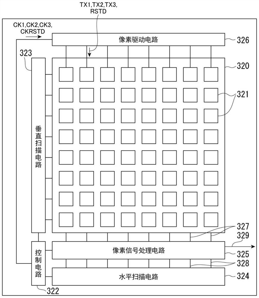
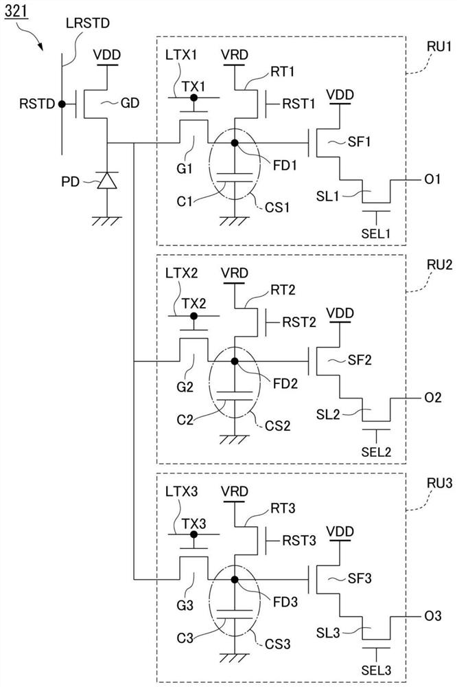
[0118] In general, in order to accurately measure the distance to the subject in the distance image sensor, all the pixel circuits 321 in the light-receiving pixel unit 320 are driven at the same timing within the accumulation period in accordance with the global shutter method. That is, each of the accumulation drive signals TX1 , TX2 , and TX3 and the reset drive signal RSTD is supplied to all the pixel circuits 321 arranged in a grid pattern at the same timing.

[0119] Therefore, for example, the peak current is transiently increased and greatly increased so that the gates of the readout gate transistors G1 of all the pixel circuits 321 in the light-receiving pixel unit 320 are at the "H" level at the same timing. Due to the transient increase of the peak current, the above-described ringing occurs, and the individual charges from the pixel circuits 321 cannot be accurately read out. The above-mentioned problem also arises when the other storage drive signals TX1 , TX2 , a...

no. 2 approach

[0175] Hereinafter, a second embodiment of the present invention will be described with reference to the drawings. Figure 10 It is a diagram illustrating a configuration example of a pixel driving circuit 326 that drives the pixel circuits 321 in units of columns among the pixel circuits 321 arranged in a grid in the light-receiving pixel unit 320 in the present embodiment. exist Figure 5 In the case of the above embodiment, the group of the timing adjustment circuit 326C_j and the driver circuit 326D_j in the pixel driving circuit 326 is divided into two equal groups G1 and G2. On the other hand, in the present embodiment, the group of the timing adjustment circuit 326C_j and the driver circuit 326D_j in the pixel driving circuit 326 is divided into three or more groups.

[0176] In this embodiment, in the timing adjustment circuit 326C_j and the driver circuit 326D_j group forming each group, the timing adjustment circuit 326C_j connected in series within the group suppli...

no. 3 approach

[0183] Hereinafter, a third embodiment of the present invention will be described with reference to the drawings. Figure 11 It is a diagram illustrating a configuration example of a pixel driving circuit 326 that drives the pixel circuits 321 in units of columns among the pixel circuits 321 arranged in a grid in the light-receiving pixel unit 320 in the present embodiment.

[0184] In this embodiment, the driver circuits 326D_j in the driver unit 326D of the pixel drive circuit 326 are divided into a plurality of groups, for example, n groups, and each group is provided with one timing adjustment circuit 326C_n (n is the number of groups). Therefore, the input terminals of the driver circuits 326D_j in each group are connected in a common manner through the connection point Q, and the corresponding timing adjustment circuit C_n supplies the clock signal CK to each of the driver circuits 326D_j in each group at the same timing. For example, in the case of group Gk (1≤k≤n), the...


PUM


Abstract

This range image sensor is provided with: light receiving pixel units that comprise a charge accumulation unit, which accumulates charge, and a photoelectric conversion element, which receives reflected light and generates a charge corresponding to the received reflected light, wherein said reflected light is obtained by emitting light pulses with the same pulse width at a prescribed period from a prescribed light source into a measurement space, which is the space to be measured, and the light pulses being reflected and emitted from a subject in the measurement space, and wherein pixel circuits, which accumulate charge in the charge accumulation units synchronously with irradiation of the light pulses, are arranged in a two-dimensional grid; and a pixel drive circuit that supplies to each of the pixel circuits an accumulation drive signal for accumulating charge from the photoelectric conversion element to the charge accumulation unit. The pixel drive circuit supplies the accumulation drive signal while shifting by a preset adjustment time between pixel circuits, and charge is accumulated in each of the pixel circuits from the photoelectric conversion element to the charge accumulation unit.

Description

technical field [0001] The invention relates to a range image sensor and a range image shooting device. Background technique [0002] Conventionally, time-of-flight (TOF, hereinafter referred to as "TOF") for measuring the distance between a measuring device and an object has been realized based on the time-of-flight of light in space (measurement space) by utilizing the fact that the speed of light is known. ) distance sensor. In the distance sensor of the TOF method, light (for example, near-infrared light, etc.) pulses are irradiated to the space of the measurement object (measurement space), and the time between the light pulse irradiation and the light pulse reflected by the object in the measurement space ( reflected light), that is, the distance between the measuring device and the subject is measured based on the flight time of light between the measuring device and the subject. [0003] In addition, in recent TOF distance sensors, like solid-state imaging devices ...

Claims


Application Information

Patent Timeline
Patent Type & Authority Applications(China)
IPC IPC(8): G01S7/4861G01S7/4865G01S17/89H01L27/146H04N5/353
CPCG01S17/89H01L27/146H01L27/14636G01S7/4863G01S17/894G01S7/4861G01S7/4865H04N25/745H04N25/771
Inventor 泽本岳秀
Owner 布鲁克曼科技株式会社
Learn More