Display driving circuit
a technology of driving circuit and display, applied in the field of display driving circuit, can solve the problems of reducing the power supply voltage and the possibility of erroneous operation, and achieve the effect of suppressing the peak curren
- Summary
- Abstract
- Description
- Claims
- Application Information
AI Technical Summary
Benefits of technology
Problems solved by technology
Method used
Image
Examples
first embodiment
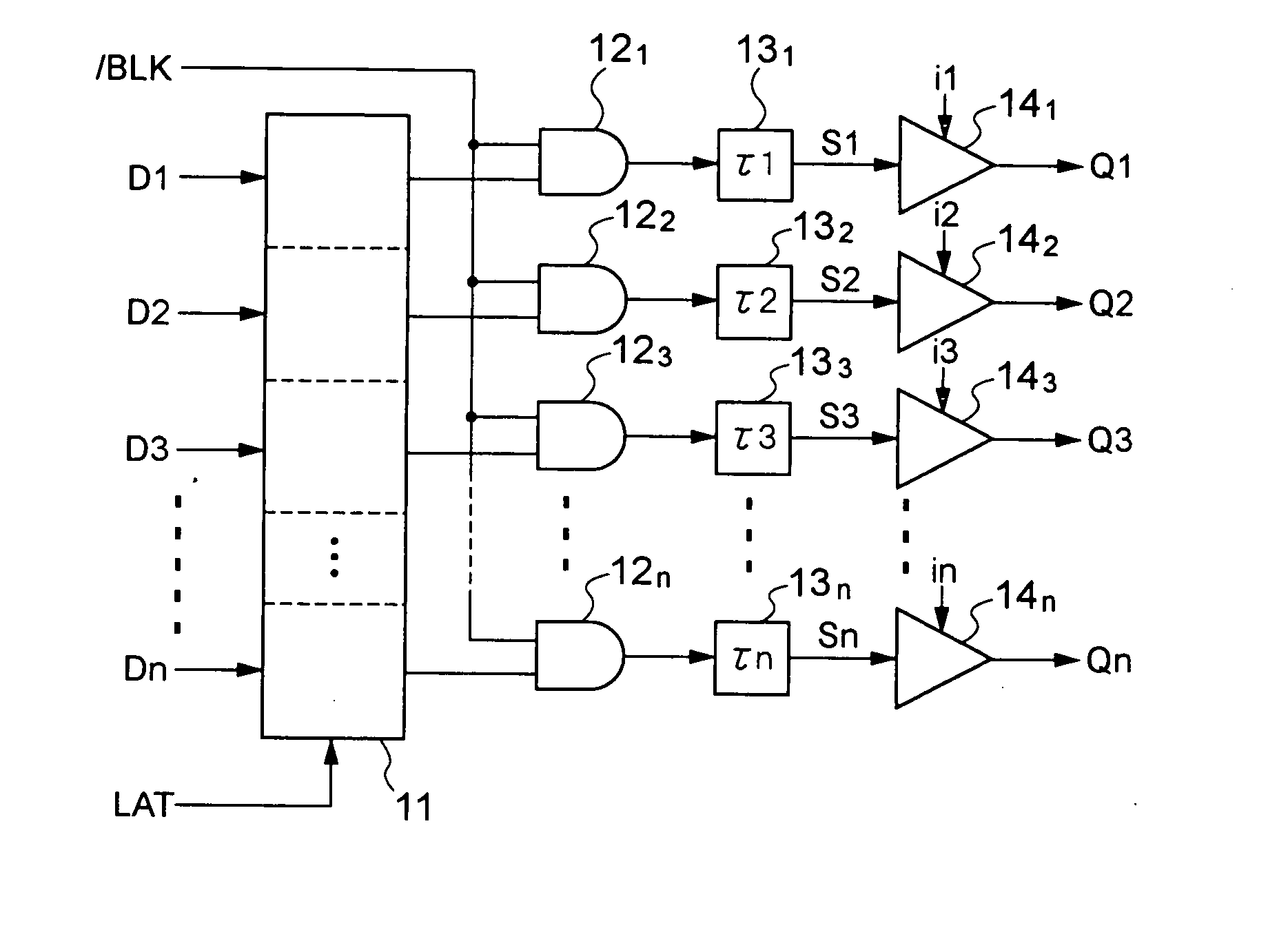
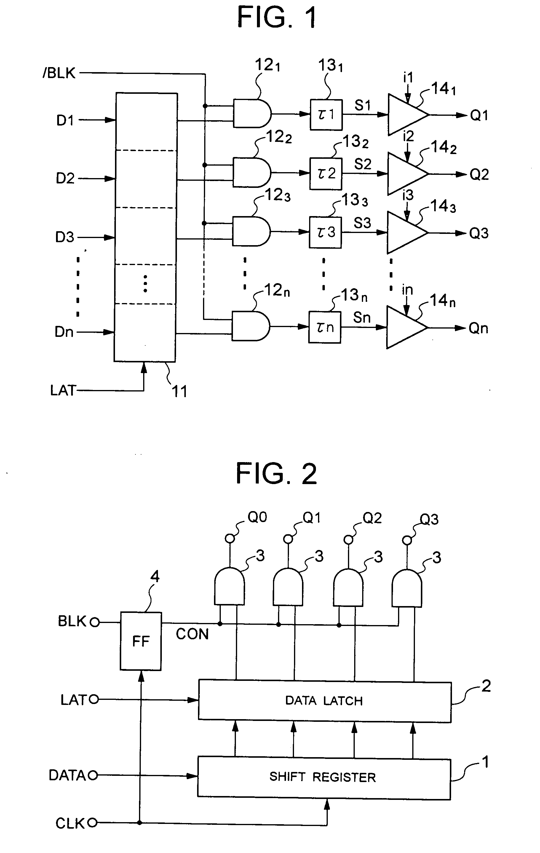
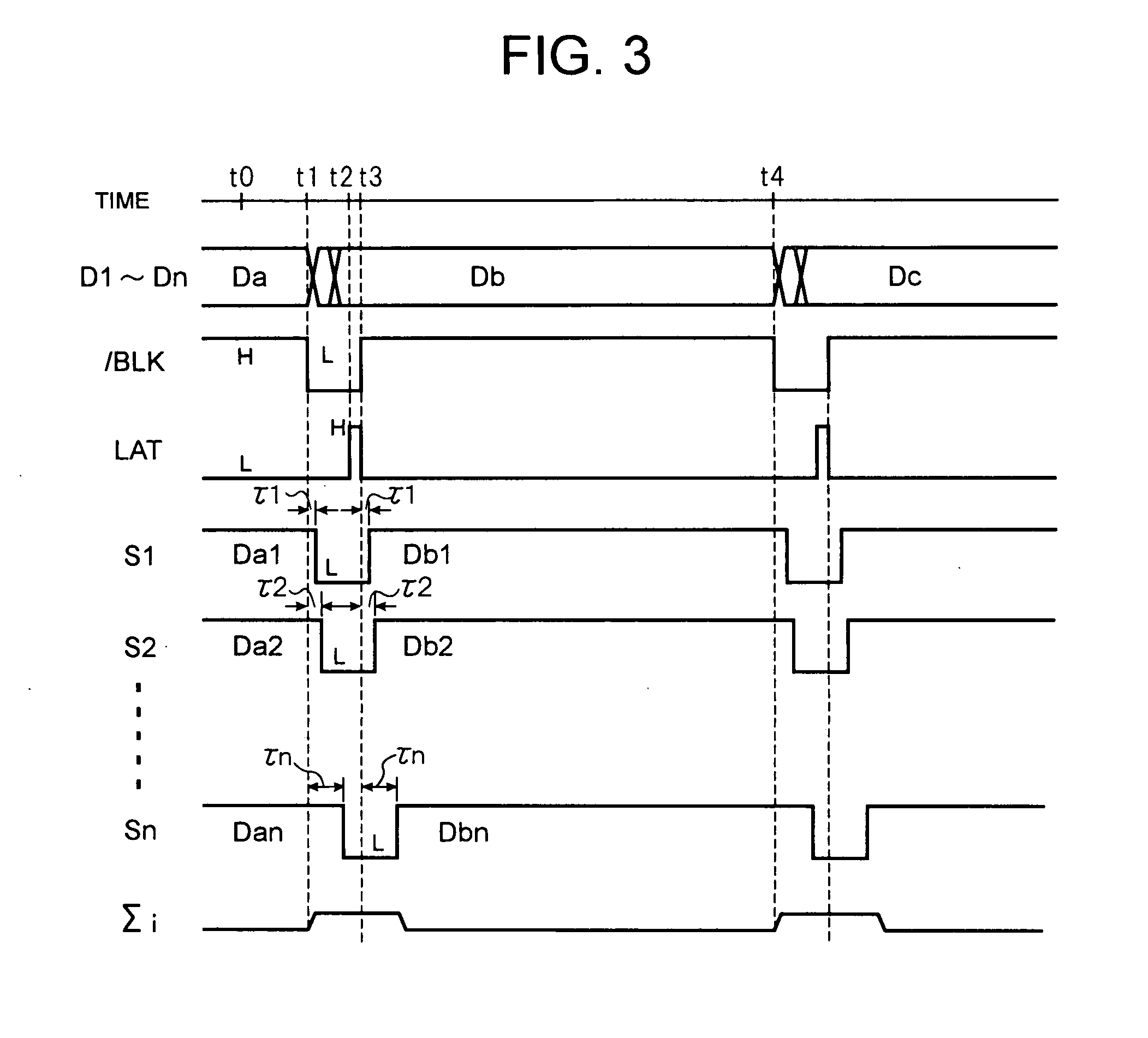
[0021] A display driving circuit shown in FIG. 1 drives a fluorescent display tube, liquid crystal display or the like. The display driving circuit has a holding circuit (for example, a data latch) 11 for capturing display data D1, D2, . . . and Dn, which are supplied in parallel, in response to a latch signal LAT. The data latch 11 captures and outputs the display data D1 to Dn in parallel when the latch signal LAT is “H”. When the latch signal LAT becomes “L”, the data latch 11 continues to output the signals without modification which have been captured during the latch signal LAT being “H”.
[0022] The outputs of the data latch 11 are respectively connected to AND gates 121, 122, . . . and 12n which are gate-controlled by a common blanking signal / BLK. Specifically, the AND gates 121 to 12n always output “L” when the blanking signal / BLK is “L” regardless of the output signal from the data latch 11, whereas the AND gates 121 to 12n output the output signals from the data latch 11...
second embodiment
[0040]FIG. 4 is a configuration of a display driving circuit according to a second embodiment of the present invention. The same reference numerals are assigned for the same elements as in FIG. 1.
[0041] In this display driving circuit, the delay circuits 131 to 13n of FIG. 1 are deleted, and the drivers 141 to 14n are connected to the output sides of the AND gates 121 to 12n. In addition, the blanking signal / BLK is supplied to these AND gates 121 to 12n after respective time delays by means of a delay circuit. The delay circuit consists of delay buffers 151, 152, . . . and 15n-1 having the same circuit configurations and connected in series. Specifically, the blanking signal / BLK is supplied to the AND gate 121. The blanking signal / BLK is supplied to the AND gate 122 via the delay buffer 151 providing a delay of τ. The blanking signal / BLK is supplied to the AND gate 123 via the delay buffers 151 and 152 providing a delay of 2τ. Subsequently, a blanking signal is supplied in a sim...
third embodiment
[0053]FIG. 5 is a configuration of a delay buffer according to a third embodiment of the present invention.
[0054] This delay buffer is provided in place of each of the delay buffers 151 to 15n-1 of FIG. 4. It should be noted that one delay buffer 151 (1≦i≦n−1) is shown in FIG. 5. Basically the delay buffer has a primary inverter stage and last inverter stage connected in series. The primary inverter stage is configured with two inverters connected in parallel, such that a control signal is used to electrically disconnect one of the inverters so as to control the time delay.
[0055] Specifically, the primary inverter stage includes a first CMOS inverter. The first CMOS inverter has PMOS (P channel MOS) transistors 21 and 22 connected in series between the power supply potential VDD and a node N1 and NMOS (N channel MOS) transistors 23 and 24 connected in series between this node N1 and the ground potential GND. The control signal CON and the control signal / CON, which is an inversion...
PUM
 Abstract
Description
Claims
Application Information


