
Gate drive circuit

A gate drive circuit and gate drive technology, applied in the field of gate drive circuits and active matrix displays, can solve the problems of high power loss, circuit burnout, etc., to avoid power loss, suppress the occurrence of large peak current, avoid The effect of circuit burnout

Active Publication Date: 2012-02-15
AU OPTRONICS CORP
View PDF0 Cites 0 Cited by
  • Summary
  • Abstract
  • Description
  • Claims
  • Application Information

AI Technical Summary

Problems solved by technology

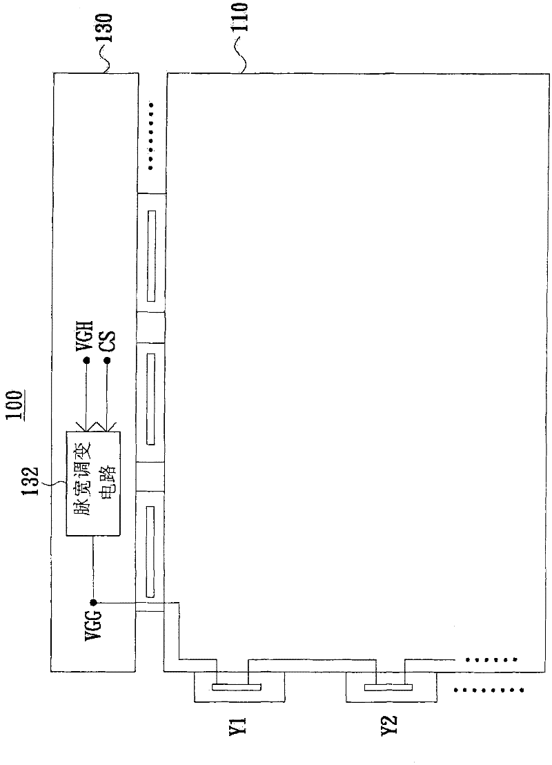
[0003] However, in the process of modulation of the gate supply voltage VGH into the modulated voltage signal VGG, since the cascade-coupled gate drive integrated circuits Y1 and Y2 use the modulated voltage signal VGG provided by the same pulse width modulation circuit 132 as the power supply Voltage, and the potential of the modulated voltage signal VGG changes periodically, when the potential of the modulated voltage signal VGG is cut from the gate power supply voltage VGH to a lower level and then pulled back to the gate power supply voltage VGH, the pulse width modulation A discharge current formed in the transformer circuit 132 will increase sharply and a large peak current (high peak current) will appear, resulting in a large power loss and even burning the circuit

Method used


Image

  • Gate drive circuit
  • Gate drive circuit
  • Gate drive circuit

Examples


Embodiment Construction

[0048]In order to make the above and other objects, features and advantages of the present invention more comprehensible, preferred embodiments are specifically cited below and described in detail with accompanying drawings.

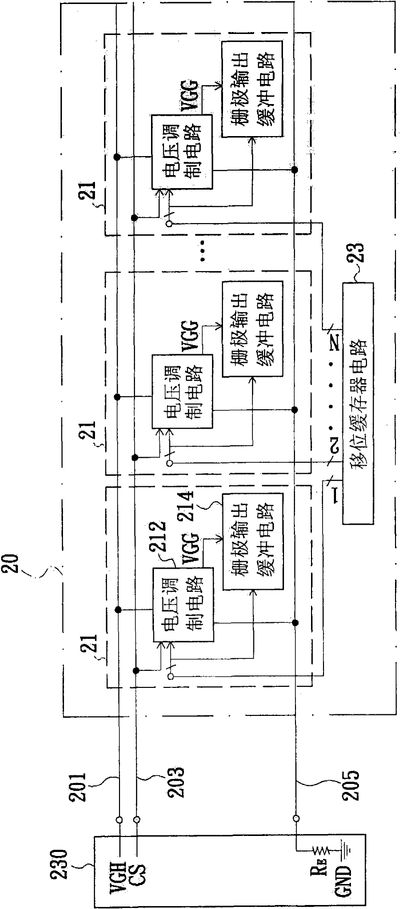
[0049] see figure 2 , a gate driving circuit 20 provided by an embodiment of the present invention is electrically coupled to a printed circuit board 230 . Wherein, the printed circuit board 230 is used to provide the gate driving circuit 20 with the gate power supply voltage VGH, the control signal CS and a predetermined potential such as the ground potential GND. The gate drive circuit 20 includes a gate power supply voltage input line 201, a control signal input line 203, a preset potential input line 205, a plurality of gate signal generation modules 21, and a shift register circuit 23; the gate power supply voltage input line 201 receives the gate power supply voltage VGH due to the electrical coupling relationship, the control signal input line 2...


PUM


Abstract

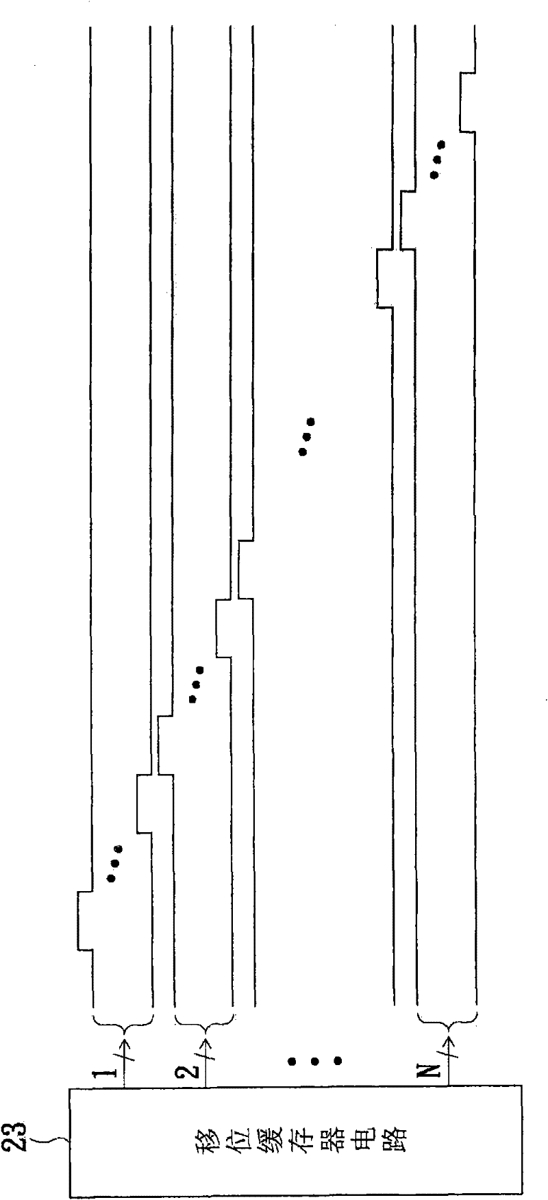
The invention discloses a gate driving circuit, which is suitable for receiving an external gate power supply voltage and an external control signal, generating a plurality of internal shift data signal groups in sequence, and The internal shift data signal group outputs a plurality of gate signals in sequence, and each internal shift data signal group includes a plurality of sequentially generated internal shift data signals; and the gate driving circuit includes a plurality of gate signal generating modules, And each gate signal generating module includes a voltage modulation circuit and a gate output buffer circuit. The voltage modulation circuit uses the corresponding ones in the internal shift data signal group and the external control signal to modulate the external gate power supply voltage to obtain a modulated voltage signal; the gate output buffer circuit includes a plurality of output stages coupled in parallel, these output stages are sequentially enabled to output modulated voltage signals to obtain some of the above gate signals. The gate driving circuit of the embodiment of the present invention can effectively suppress the occurrence of large peak current, avoid unnecessary power loss and / or avoid circuit burnout.

Description

technical field [0001] The invention relates to the field of display technology, in particular to a gate drive circuit, which is suitable for application in active matrix displays. Background technique [0002] see figure 1 , which is a structural block diagram of an existing active matrix display. Such as figure 1 As shown, the active matrix display 100 includes a display substrate 110, a printed circuit board 130, a plurality of source driver integrated circuits (not shown) electrically coupled between the display panel 110 and the printed circuit board 130, and includes a plurality of The gate driving circuits of the gate driving integrated circuits Y1 and Y2 are cascadedly coupled. Wherein, a thin film transistor array (not shown) is formed on the display substrate 110, and the gate driving integrated circuits Y1 and Y2 in the gate driving circuit are electrically coupled to the thin film transistor array of the display substrate 110 as switches for each thin film tra...

Claims


Application Information

Patent Timeline
Patent Type & Authority Patents(China)
IPC IPC(8): G09G3/20
Inventor 黄文江汪志松何宇玺
Owner AU OPTRONICS CORP
Learn More