PFR flash memory expansion device and method
A technology of expansion device and flash memory, which is applied in the field of servers, can solve problems such as insufficient space and inability to support, and achieve the effects of simple structure, wide application prospects, and reliable design principles
- Summary
- Abstract
- Description
- Claims
- Application Information
AI Technical Summary
Problems solved by technology
Method used
Image

Examples
Embodiment 1
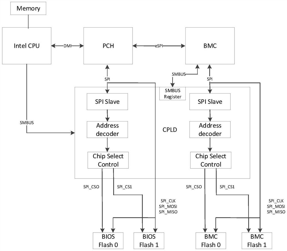
[0048] In the existing PFR flash memory architecture, both BMC and BIOS are suitable for configuring a Flash, and communicate with the Flash through the SPI interface. The CPLD is mainly responsible for the basic functions of PFR through the SPI interface, the three major functions of Detection, Protection and Recovery. If the BMC or BIOS adds additional functions, resulting in insufficient Flash space, usually the number of Flash will be increased for expansion. Since the PFR firmware provided by Intel does not include an expansion mechanism, BIOS and BMC need to develop additional firmware to control more than two Flash. At the same time, the CPLD PFR function also needs to cooperate with BIOS and BMC at the same time.
[0049] Please refer to figure 1 , this embodiment provides a PFR flash memory expansion device, including:
[0050] A programmable logic device, a paging channel and a baseboard management controller, the paging channel is used to transmit instructions of ...
Embodiment 2
[0056] This embodiment provides a PFR flash memory expansion device, including:
[0057] A programmable logic device, a paging channel and a baseboard management controller, the paging channel is used to transmit instructions of the BIOS in the CPU. The paging channel is connected to the programmable logic device through the SPI first signal link, and the programmable logic device is respectively connected to the first flash memory, the second flash memory and the third flash memory through the SPI first signal link; the paging channel The first flash memory, the second flash memory and the third flash memory are respectively connected to the first flash memory, the second flash memory and the third flash memory through the second signal link of SPI; the baseboard management controller is connected to the programmable logic device through the first signal link of SPI, and the programmable logic device is The first signal link is respectively connected to the fourth flash memor...
Embodiment 3
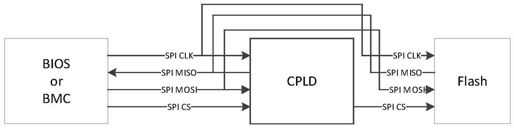
[0061] Please refer to figure 2 , the present embodiment provides a PFR flash memory expansion method, comprising the following steps:
[0062] S1. The programmable logic device receives the SPI_CSO signal sent by the server management device and decodes the SPI_CSO signal.
[0063] The SPI Slave module of CPLD receives the SPI_CSO signal sent by BMC or BIOS, and decodes the received SPI_CSO signal according to the SPI protocol standard.
[0064] S2. Analyze the target flash memory from the decoded SPI_CSO signal.
[0065] The Address decoder module parses the SPI_CSO signal and obtains the source server management device information (BMC or BIOS), searches for all flash memories connected to the source server management device according to the source server management device information as candidate objects; selects the target flash memory from the candidate objects memory as the target flash memory. Obtain the memory required by the task from the analyzed SPI_CSO signal;...
PUM
 Abstract
Description
Claims
Application Information